Light-emitting device, planar light source including the light-emitting device, and liquid crystal display device including the planar light source

a liquid crystal display and light-emitting technology, which is applied in the direction of lighting and heating apparatus, instruments, optical elements, etc., can solve the problems of resin packaging that cannot meet the demand for cost reduction with this technique, the resin package cannot handle the need for a higher intensity light source becomes necessary with the increase in the size of the liquid crystal backlight device, etc., to achieve excellent light uniformity, good heat dissipation

Active Publication Date: 2011-03-03
SHARP KK
View PDF10 Cites 52 Cited by
  • Summary
  • Abstract
  • Description
  • Claims
  • Application Information

AI Technical Summary

Benefits of technology

[0049]According to the above configuration, since the planar light source having good heat dissipation properties and excellent light uniformity is used as a backlight, the liquid crystal display device that can perform uniform display with high accuracy can be achieved.

Problems solved by technology

However, a higher-intensity light source becomes necessary with an increase in the size of a liquid crystal backlight device.
Here, although it is possible to consider using many LEDs as a technique for increasing the intensity of a light source, it will be difficult to satisfy the demand for cost reduction with this technique.
However, a resin package as disclosed in Patent Document 1 has a problem that such a resin package cannot handle an increase in the size of a liquid crystal backlight device since its heat dissipation properties and heat resistance properties are insufficient.
Further, a ceramic package as disclosed in Patent Document 2 has a problem that although such a ceramic package has higher heat conductivity compared to the resin package, it cannot be said that its heat dissipation properties are sufficient.

Method used


Image

  • Light-emitting device, planar light source including the light-emitting device, and liquid crystal display device including the planar light source
  • Light-emitting device, planar light source including the light-emitting device, and liquid crystal display device including the planar light source
  • Light-emitting device, planar light source including the light-emitting device, and liquid crystal display device including the planar light source

Examples


embodiment 1

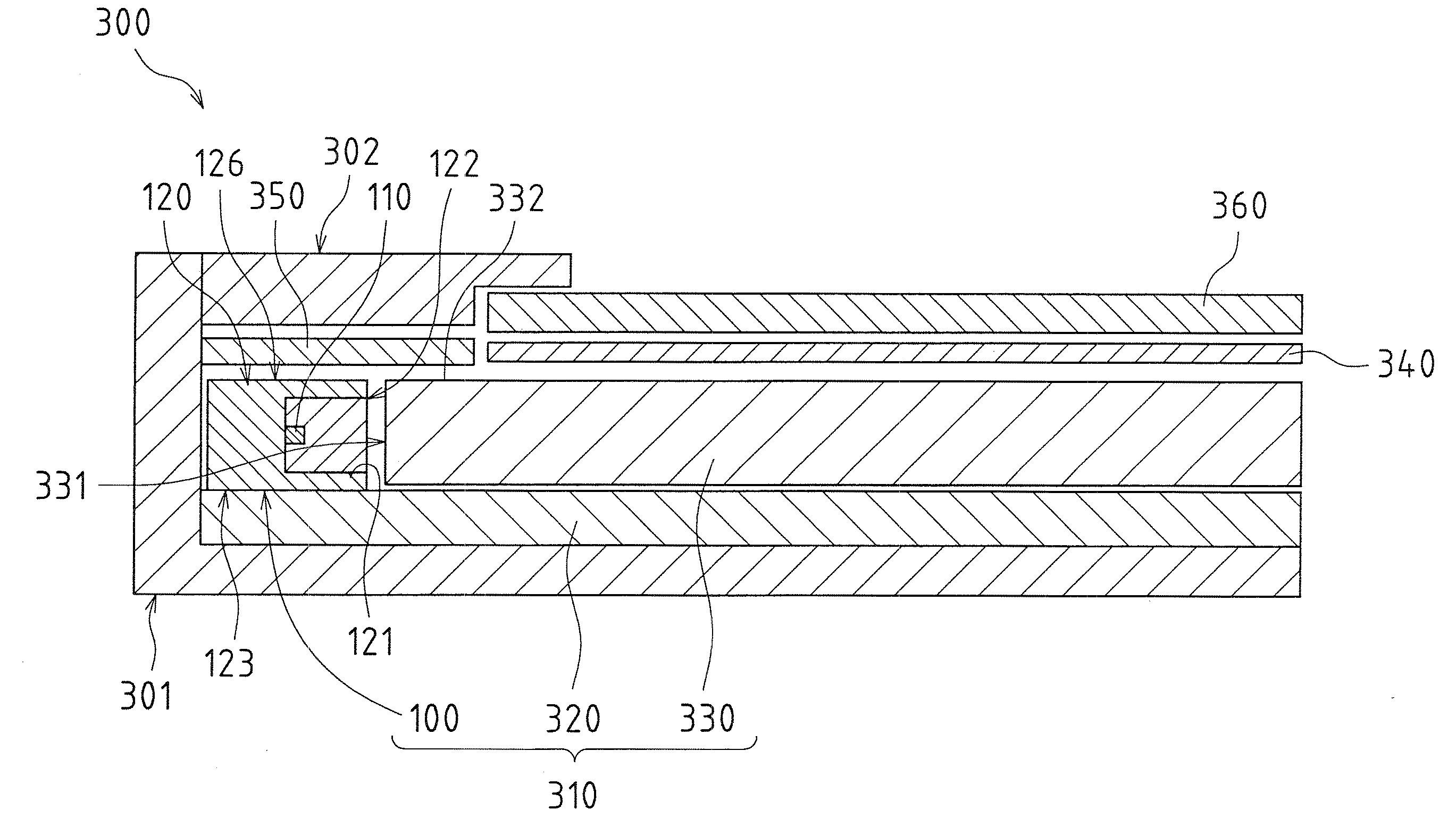
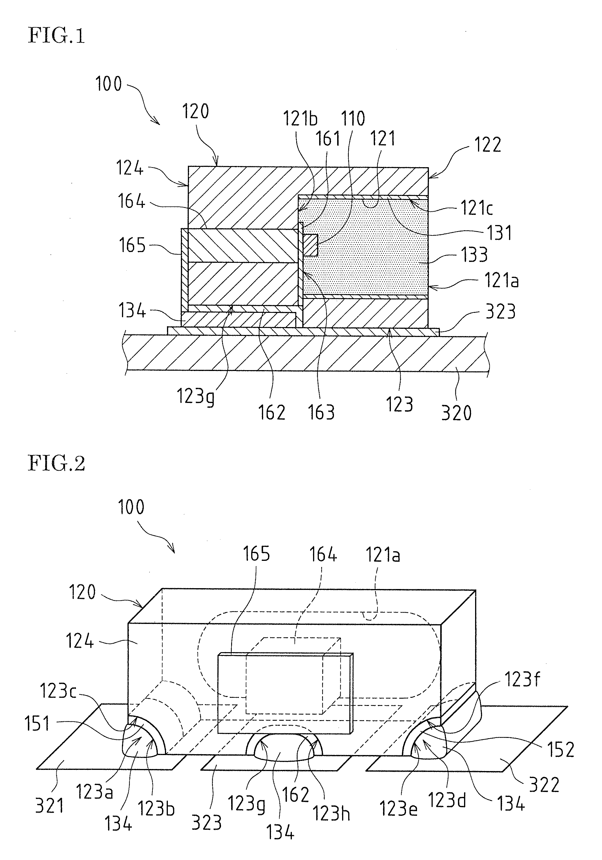
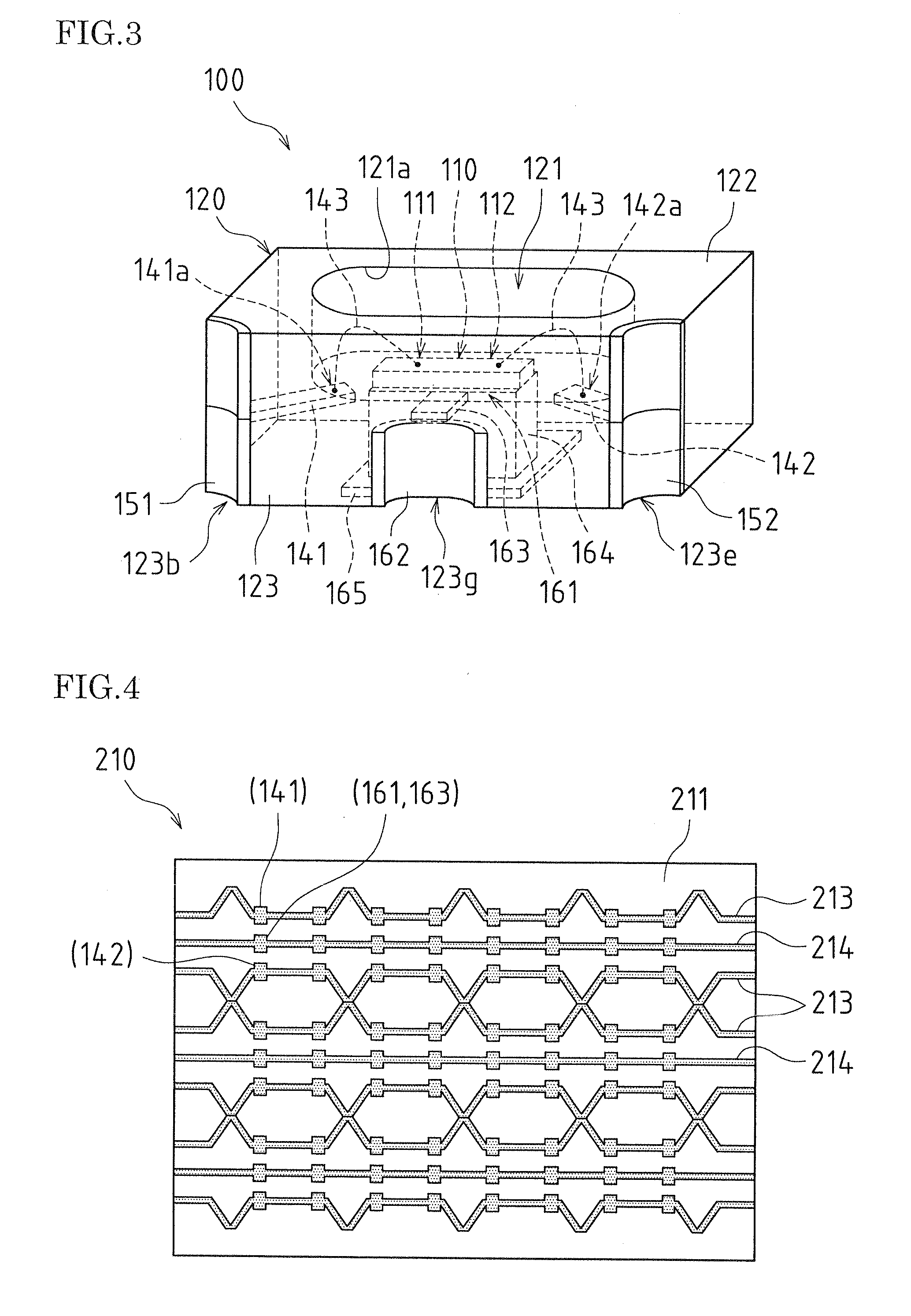
[0069]A light-emitting device according to Embodiment 1 of the present invention is described with reference to FIGS. 1 to 3.

[0070]FIG. 1 is a cross-sectional view showing the light-emitting device according to Embodiment 1 of the present invention. FIG. 2 is a perspective view conceptually showing the light-emitting device according to Embodiment 1 that is seen obliquely from above. FIG. 3 is a perspective view conceptually showing the light-emitting device according to Embodiment 1 that is seen obliquely from below. Note that FIGS. 1 and 2 show, for convenience, a part of a mounting substrate on which the light-emitting device is mounted.

[0071]A light-emitting device 100 according to Embodiment 1 is provided with an LED chip 110 and a ceramic substrate 120. The light-emitting device 100 is mounted on land patterns 321, 322, and 323 formed on a mounting substrate 320. The light-emitting device 100 is constituted as a side light-emitting type light-emitting device, and emits light f...

embodiment 2

[0123]A method for manufacturing a light-emitting device according to Embodiment 2 of the present invention is described with reference to FIGS. 4 to 12. Note that with regard to the items in common with Embodiment 1, the same reference numerals are employed where appropriate.

[0124]In Embodiment 2, a description is given on a procedure of manufacturing the light-emitting device 100 according to Embodiment 1 using two green sheet groups (a first green sheet group 210 formed by laminating four green sheets, and a second green sheet group 230 formed by laminating four green sheets). The first green sheet group 210 and the second green sheet group 230 are laminated and fired so as to form a ceramic substrate 200 in an aggregate state (state in which a large number of the ceramic substrates 120 are simultaneously formed), which serves as the base material of the ceramic substrate 120.

[0125]FIG. 4 is a plan view schematically showing conceptual disposition, with respect to a face 211, of ...

embodiment 3

[0149]A light-emitting device according to Embodiment 3 of the present invention is described with reference to FIGS. 13 and 14. Note that with regard to the items in common with Embodiments 1 and 2, the same reference numerals are employed where appropriate.

[0150]FIG. 13 is a cross-sectional view schematically showing a light-emitting device according to Embodiment 3 of the present invention. FIG. 14 is a lateral view of the light-emitting device shown in FIG. 13 seen from the opening face side.

[0151]Although a light-emitting device 100A according to Embodiment 3 has substantially the same configuration as that of the light-emitting device 100 according to Embodiment 1, the difference from the light-emitting device 100 according to Embodiment 1 is that a difference in level is provided between the placement face 121b on which the LED chip 110 is placed and an internal terminal plane 140 constituted by the internal anode terminal 141 and the internal cathode terminal 142.

[0152]In th...


PUM

PropertyMeasurementUnit
wavelengthaaaaaaaaaa
heat conductionaaaaaaaaaa

Abstract

A light-emitting device according to an embodiment of the present invention includes a light-emitting element, and a package substrate on which this light-emitting element is placed. This package substrate includes a placement face on which the light-emitting element is placed, a back face that is opposed to the placement face, and a mounting face that is opposed, between the placement face and the back face, to a mounting substrate when the light-emitting device is mounted, and includes a first recess portion that extends, on the mounting face, from the back face toward the placement face and that has a first heat conduction member formed on the surface thereof, and an intermediate heat conduction member for conducting heat between the light-emitting element and the first heat conduction member.

Description

CROSS-REFERENCE TO RELATED APPLICATION[0001]This application claims priority under 35 U.S.C. §119(a) on Patent Application No. 2009-201908 filed in Japan on Sep. 1, 2009, the entire contents of which are herein incorporated by reference.BACKGROUND OF THE INVENTION[0002]The present invention relates to a light-emitting device, a planar light source, and a liquid crystal display device.[0003]LEDs (light-emitting diodes) have been widely used along with the improvement in their efficiency in recent years as a more energy-saving light source than electric bulbs and fluorescent lamps. In recent years, development of blue LEDs has been making progress, and white LEDs achieved by using a combination of a blue LED and a fluorescent material are also in practical use. White LEDs are being used as a light source for the small liquid crystal backlight devices of mobile terminals and the like. In particular, a liquid crystal backlight device using a side light-emitting type light-emitting devic...

Claims


Application Information

Patent Timeline
Patent Type & Authority Applications(United States)
IPC IPC(8): G02F1/1335H01L33/48F21V7/22
CPCG02B6/0083H01L2224/48464H01L33/62H01L33/642H01L33/647H01L33/486H01L2224/48228H01L24/97H01L2924/01006H01L2224/48227H01L2924/01047H01L2924/01015H01L2924/12041H01L24/45H01L2224/45H01L2224/48091H01L2924/00014H01L2924/00H01L2924/00011H01L2924/15787H01L2924/181H01L24/48H01L2224/45099H01L2224/43H01L2924/00012
Inventor OKAMOTO, KAZUHIROKONISHI, MASAHIROKITANO, MASAHARU
Owner SHARP KK
Why Eureka
Try Eureka