
Method for high-temperature ceramic circuits

a ceramic circuit and high-temperature technology, applied in the direction of superimposed coating process, resistive material coating, liquid/solution decomposition chemical coating, etc., can solve the problem of prone failure of the temperature cycling of the ltcc assembly, and achieve the effect of reducing the aging process

Inactive Publication Date: 2011-03-03
NORMANN RANDY ALLEN +1
View PDF8 Cites 2 Cited by
  • Summary
  • Abstract
  • Description
  • Claims
  • Application Information

AI Technical Summary

Benefits of technology

[0013]Plasma (electrical arc) spray, flame spray or high velocity impact processes can be used to create metal surfaces on ceramic without organic materials or high-temperature co-firing. As such, this process allows the use of completely fired ceramic before placing the conductive traces onto the board. This also allows the use of any type of ceramic, even very high-temperature ceramic such as silicon-carbide. Once the ceramic is coated with a layer of conductive metal, it can be worked like any standard circuit board material. In standard (very low cost) circuit board manufacturing unwanted metal is removed using a chemical process. However, any machining process could also be used.
[0016]1. Plasma (electrical arc) spray, flame spray or high velocity impact processes are faster and less expensive than silk screening used in the LTCC process.
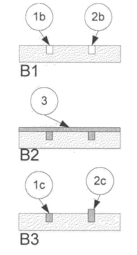
[0017]2. Placing conductive metal traces in etched ceramic allows for the metal to attach to the ceramic on three sides. Such a configuration allows higher bonding strengths between the ceramic and the metal traces allowing for improve operating life times for applications with temperature cycling. Greater bonding allows for heavier metallization for improved current carrying capability.
[0018]3. Placing the metal on the ceramic after the ceramic is fired allows for unlimited board and trace sizes.
[0020]5. By eliminating any organic material from the circuit, significantly reduces the aging process when operated at temperatures over 200° C. At elevated temperatures, organic materials break down or decompose.

Problems solved by technology

So, during high-temperature circuit operations the temperature cycling of the LTCC assembly is prone to failure.

Method used


Image

  • Method for high-temperature ceramic circuits
  • Method for high-temperature ceramic circuits

Examples


Embodiment Construction

[0024]This invention allows for the creation of electronic circuits to be manufactured as electrically conductive recesses in a non-conductive material as ceramic.

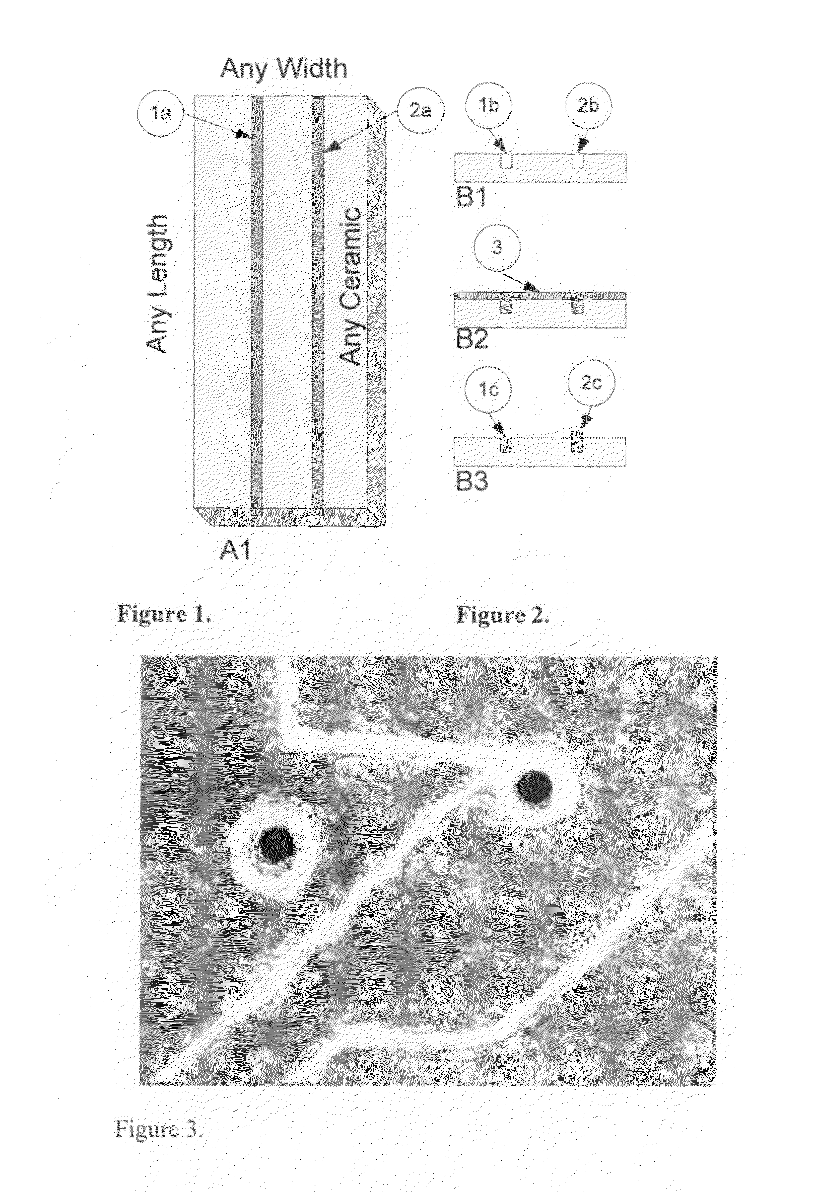
[0025]Under work conducted at Sandia National Labs by the inventors Joseph Henfling and Randy Normann, the process of creating a metal layer onto a clean ceramic surface was demonstrated as illustrated in FIG. 1.

[0026]FIG. 1 illustrates that there are no size limitations in length, width of the conductive traces. Our process allows for the metal conductor to be placed on the ceramic after the ceramic has been cured.

[0027]Under work conducted under DOE grant to Perma Works LLC, inventor Randy Normann developed the concept illustrated in FIG. 2 to commercial practice shown in FIG. 3. FIG. 2 illustrates an example creation of two conductive traces on non-electrically conductive ceramic. The invention is the construction of any number of conductive traces, mounting pads and interconnecting via within manufactured recesses in a...


PUM

PropertyMeasurementUnit
Temperatureaaaaaaaaaa
Electrical conductivityaaaaaaaaaa
Poweraaaaaaaaaa

Abstract

A novel means for placing conductive metal traces on ceramic without adhesives, glues or any organic materials. Metal traces created by thermal spraying metal on to a prepared ceramic surface. The ceramic surface is prepared by creating recesses where the metal is to remain as circuit traces. Following thermal spray, the excess metal is removed from the surface leaving the metal electrically conductive traces in the ceramic recesses. This process improves metal to ceramic bond, reducing failures caused from thermal expansion differences between ceramic and metal traces and eliminates all organic adhesives.

Description

GOVERNMENT INTERESTS[0001]Part of this invention was developed under Contract DE-AC04-94AL8500 between Sandia Corporation and the U.S. Department of Energy. The U.S. Government has certain rights in this invention.[0002]The remaining parts of this invention were developed under award number DE-FG36-08GO18185 between Perma Works LLC and the U.S. Department of Energy. The U.S. Government has certain rights in this invention.BACKGROUND OF THE INVENTION[0003]1. Technical Field of the Invention[0004]A means for creating conductive metal traces on or in ceramic for the purposes of creating electronic circuits.[0005]2. Description of Prior Art[0006]Ceramic materials have been used for building circuit boards for more than 20 years. Ceramics have a very good thermal expansion coefficient for mounting silicon chips (bare integrated circuits). As such, ceramic circuit boards are used in multi-chip-modules (MCM) to build reliable electronic circuits which can operate over a board range of temp...

Claims


Application Information

Patent Timeline
IPC IPC(8): H05K3/00
CPCH05K1/0306H05K3/0014H05K3/0044H05K3/045H05K2203/1476H05K2203/025H05K2203/1142H05K2203/1344H05K3/14
Inventor NORMANN, RANDY ALLENHENFLING, JOSEPH ANTHONY
Owner NORMANN RANDY ALLEN
Learn More