Transverse field type liquid crystal display panel

a liquid crystal display panel and transverse field technology, applied in non-linear optics, instruments, optics, etc., can solve the problems of narrow viewing angle, burnt phenomenon, and more marked burnt phenomenon, so as to reduce burnt

Active Publication Date: 2008-11-20
JAPAN DISPLAY WEST
View PDF11 Cites 35 Cited by
  • Summary
  • Abstract
  • Description
  • Claims
  • Application Information

AI Technical Summary

Benefits of technology

[0022]The inventors arrived at the present invention when they discovered, as a result of intensive and extensive investigations to alleviate the problem of burn-in with such FFS mode liquid crystal display panels, that although in FFS mode liquid crystal display panels it is problematic, due to the operating principles thereof, to render symmetrical the path of the electric field lines from the pixel electrodes to the liquid crystal layer and the path thereof from the liquid crystal layer to the scan lines; nevertheless, by ensuring that the DC field arising from the high voltage signals applied to the scan lines is not applied to the nearby liquid crystals, it is possible to reduce burn-in not only in FFS mode liquid crystal display panels but in IPS mode liquid crystal display panels also.

Problems solved by technology

Among such longitudinal field type liquid crystal display panels there exist those with a twisted nematic (TM) mode or vertical alignment (VA) mode, which however have the problem that their viewing angle is narrow.
However, it is well known that when used for prolonged periods, liquid crystal display panels are prone to the phenomenon of burn-in.
It would be undesirable for the extent of each scan line covered by the shield electrodes to be less than half, since the smaller such extent becomes, the more marked is the burn-in phenomenon.

Method used


Image

  • Transverse field type liquid crystal display panel
  • Transverse field type liquid crystal display panel
  • Transverse field type liquid crystal display panel

Examples


first embodiment

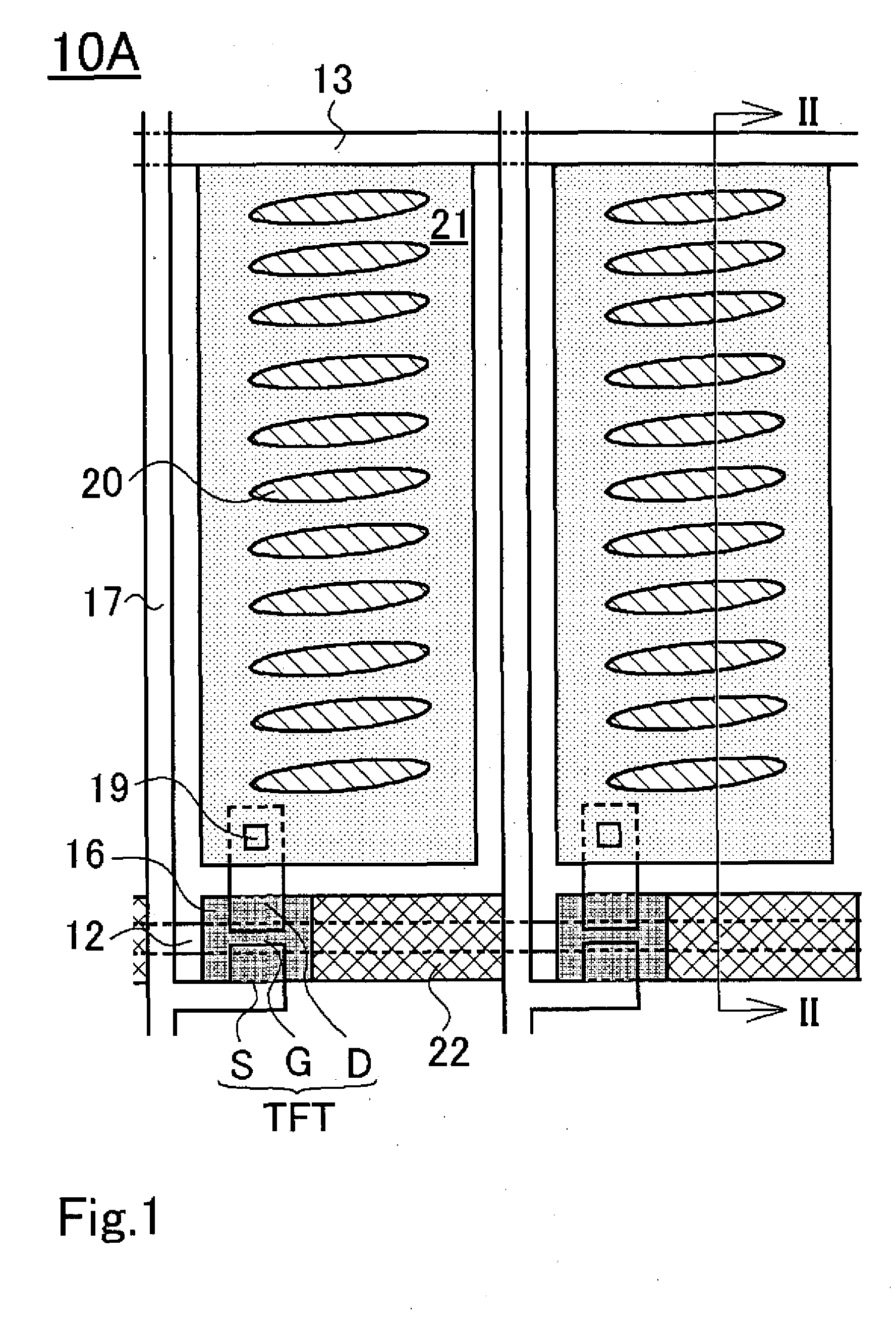
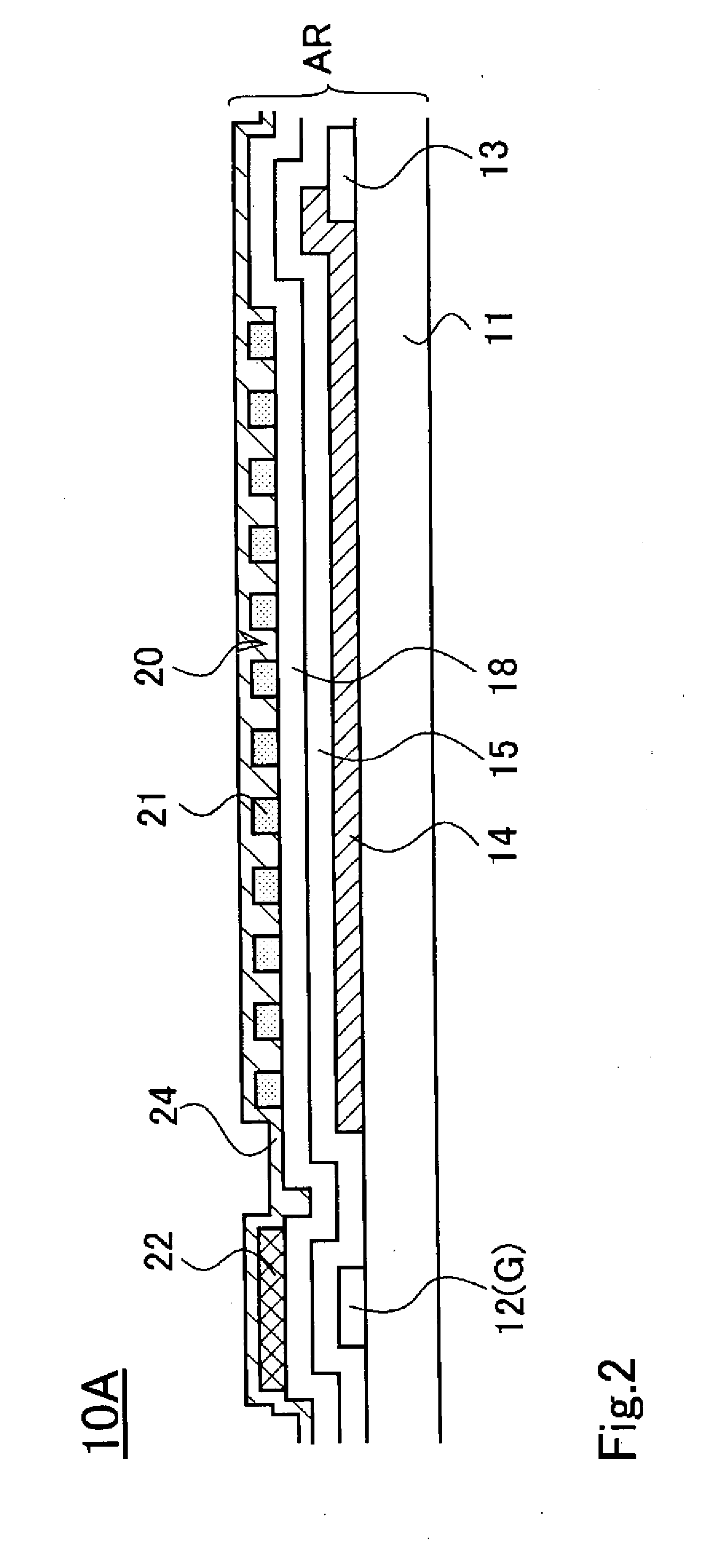
[0082]An FFS mode liquid crystal display panel 10A of a first embodiment of the invention is described below by recounting the process of its manufacture, using FIGS. 1 and 2. FIG. 1 is a schematic plan view of two pixel portions of the FFS mode liquid crystal display panel of the first embodiment, seen through the color filter substrate, and FIG. 2 is a cross-sectional view along line II-II in FIG. 1.

[0083]According to the first embodiment of the invention, an array substrate AR of the FFS mode liquid crystal display panel 10A includes a transparent substrate 11 constituted by a substrate of glass or the like, over the entire surface of which a 2-layer film composed of a lower layer of aluminum (Al) metal and a surface layer of molybdenum (Mo) metal is formed, from which film there are then formed, by photolithographic and etching methods, multiple scan lines 12 and common wires 13, lying parallel to each other and including Mo—Al 2-layer wiring lines. Aluminum has the merit that i...

second embodiment

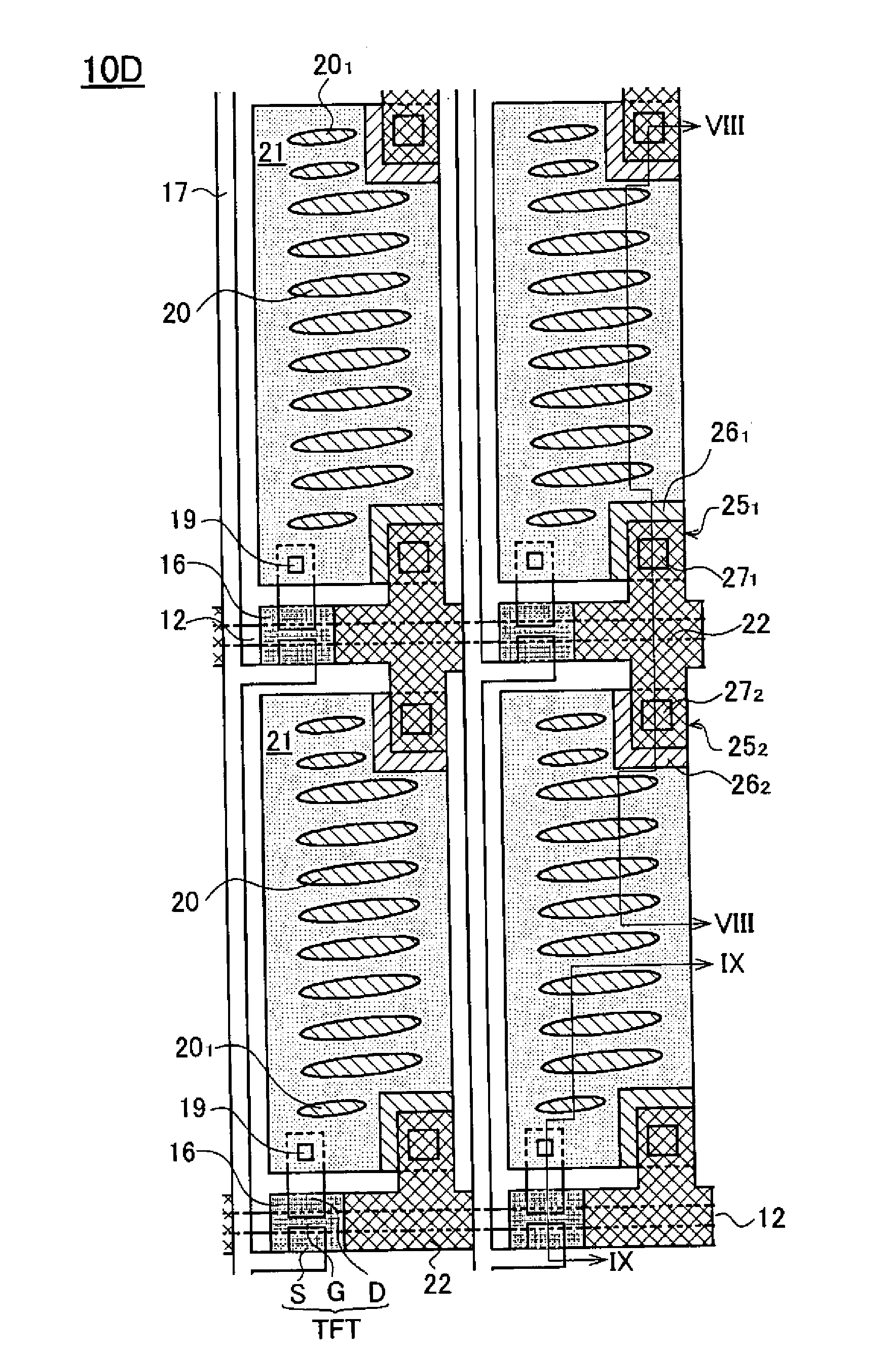
[0089]With the FFS mode liquid crystal display panel 10A of the first embodiment, the shield electrodes 22 are in a floating state, which means that the potential of the shield electrodes 22 could become unstable due to the influence of external fields, and fluctuate markedly. Accordingly, an FFS mode liquid crystal display panel 10B of a second embodiment stabilizes the potential of the shield electrodes 22 by electrically connecting the shield electrodes 22 to the common electrodes 14. Such FFS mode liquid crystal display panel 10B of the second embodiment will now be described using FIGS. 3 and 4. FIG. 3 is a schematic plan view of two pixel portions of the FFS mode liquid crystal display panel of the second embodiment, seen through the color filter substrate, and FIG. 4 is a cross-sectional view along line IV-IV in FIG. 3. Component elements in FIGS. 3 and 4 that have identical structure to those in the FFS mode liquid crystal display panel 10A of the first embodiment shown in F...

third embodiment

[0094]Whereas in the FFS mode liquid crystal display panel 10B of the second embodiment the potential of the shield electrodes 22 is stabilized by electrically connecting the shield electrodes 22 to the common electrodes 14 so as not to be affected by fields from the exterior, in an FFS mode liquid crystal display panel 10C of a third embodiment the potential of the shield electrodes 22 is stabilized by electrically connecting the shield electrodes 22 to the signal lines 17. This FFS mode liquid crystal display panel 10C of the third embodiment will now be described using FIGS. 5 and 6. FIG. 5 is a schematic plan view of two pixel portions of the FFS mode liquid crystal display panel of the third embodiment, seen through the color filter substrate, and FIG. 6 is a cross-sectional view along line VI-VI in FIG. 5. Component elements in FIGS. 5 and 6 that have identical structure to those in the FFS mode liquid crystal display panel 10A of the first embodiment shown in FIGS. 1 and 2 ar...


PUM

PropertyMeasurementUnit
DC voltageaaaaaaaaaa
conductiveaaaaaaaaaa

Abstract

A transverse field type liquid crystal display panel has multiple scan lines 12 and common wires 13 provided in parallel, multiple signal lines 17 provided in the direction crossing the scan lines 12, and common electrodes 14 and pixel electrodes 21 formed in the regions delimited by the multiple scan lines 12 and signal lines 17. At least part of the surface of an insulator laid over the scan lines 17 is covered by shield electrodes 22 constituted of a conductive material. Thanks to such structure, there can be provided a transverse field type—that is, an IPS mode or FFS mode—liquid crystal display panel that is equipped with a device for preventing burn-in due to the voltage that is applied to the scan lines.

Description

BACKGROUND[0001]1. Technical Field[0002]The present invention relates to an in-plane switching (IPS) mode or fringe field switching (FFS) mode transverse field type liquid display panel, and more particularly to an IPS or FFS mode liquid crystal display panel that is equipped with a device for preventing burn-in arising from the voltage that is applied to the scan lines.[0003]2. Related Art[0004]Recent years have seen widespread use of liquid crystal display panels not only in telecommunications equipment but in electrical equipment in general. The liquid crystal display panels that have long been in use are made up of a pair of substrates of glass or the like with electrodes and so on formed on their surfaces, and a liquid crystal layer formed between such pair of substrates. Images of various types are displayed by the application of voltage to the electrodes on the two substrates, which rearranges the liquid crystals, altering the transmittance of light therethrough. This is what...

Claims


Application Information

Patent Timeline
Patent Type & Authority Applications(United States)
IPC IPC(8): G02F1/1343
CPCG02F1/134363G02F2001/136218G02F1/136218G02F1/1343
Inventor HORIGUCHI, MASAHIROKANEKO, HIDEKIMURAI, HIDETOSHIKURASAWA, HAYATOSEGAWA, YASUO
Owner JAPAN DISPLAY WEST
Why Eureka
Try Eureka