

High concentration water pulses for atomic layer deposition
a technology of atomic layer and water pulse, which is applied in the direction of coating, chemical vapor deposition coating, metallic material coating process, etc., can solve the problem of more or less self-saturation of reaction
- Summary
- Abstract
- Description
- Claims
- Application Information
AI Technical Summary
Benefits of technology
Problems solved by technology
Method used
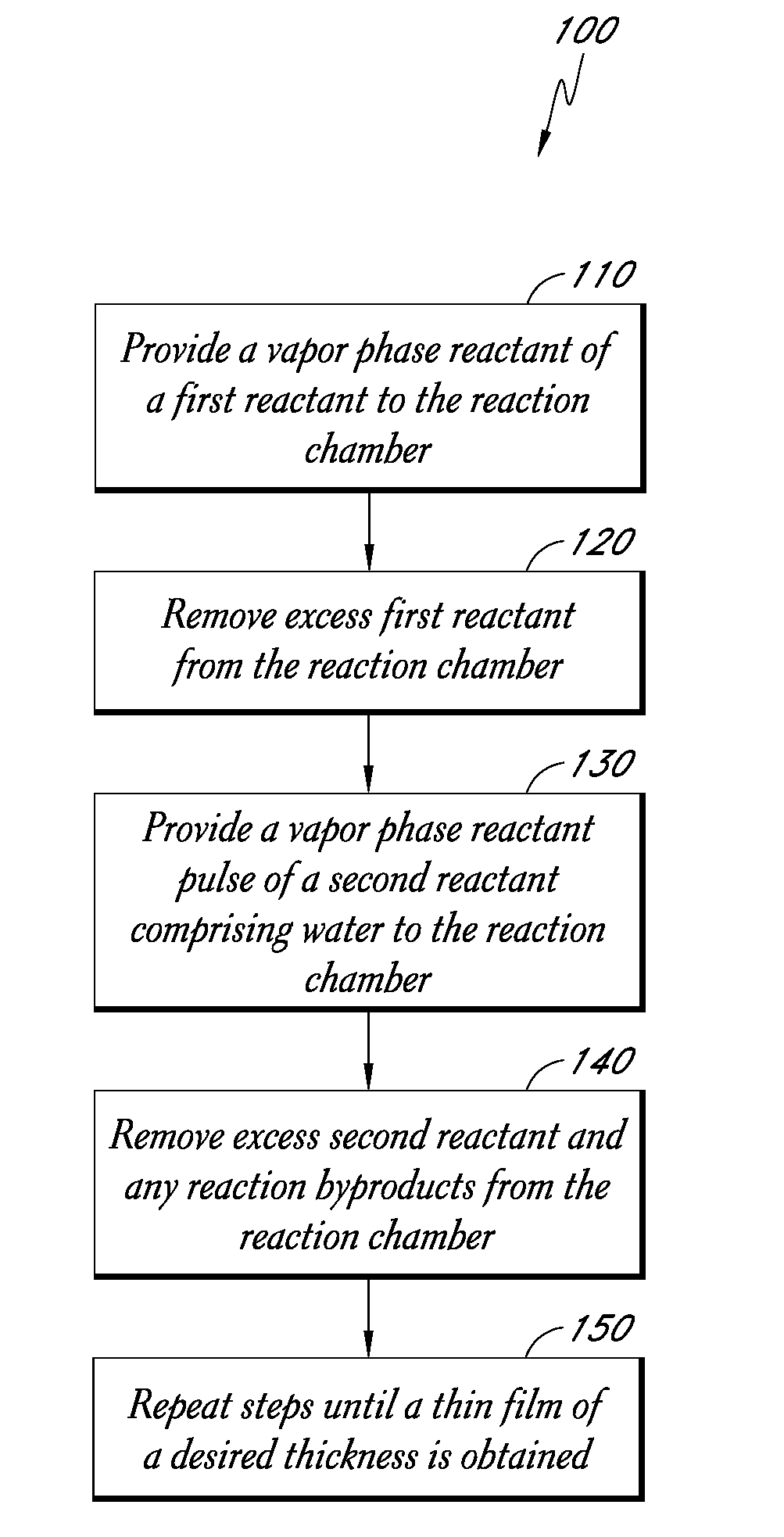
Image

Examples
example 1
[0080]A growth rate of 0.50 Å / cycle for HfO2 was achieved by ALD using alternate and sequential pulses of HfCl4 and water, with water pulse length under 500 ms in duration and the water source slightly below room temperature (15° C.). These process conditions typically result in about 15% monolayer coverage per cycle and low hydroxyl group (—OH) surface coverage.
example 2
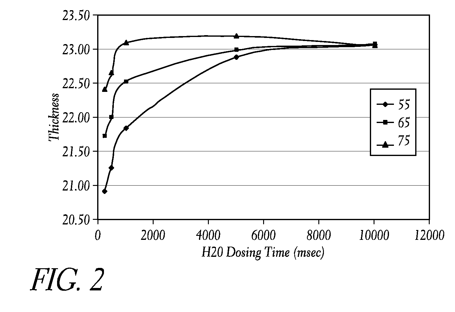
[0081]Thin films of HfO2 were deposited on a substrate by alternately and sequentially providing HfCl4 and water to a reaction space under various reactor and reactant process conditions. The substrate temperature was 300° C. FIG. 2 illustrates the effect of the water pulse time and water source temperature on the thickness of the deposited HfO2 thin film. Increasing the water pulse time from 250 ms to 5 seconds resulted in an increased film growth rate for all temperatures. Increasing the water source temperature from 55° C. to 75° C. increased the thin film growth rate. For a given pulse time, increasing the temperature of the water source vessel resulted in an increased growth rate of the HfO2 thin film. Nitrogen was used as a carrier gas.
example 3
[0082]The thin film growth rate per cycle for HfO2 films was also studied at water source vessel temperatures of 15° C., 37° C., 55° C., 65° C., and 75° C. Water and HfCl4 were used to deposit HfO2. The water pulse times were less than 1 second. The thickness of the HfO2 films was measured at various deposition cycle intervals.
[0083]The average growth rate per cycle when the water source vessel source temperature was 15° C. was 0.50 Å / cycle. The average growth rate per cycle when the water source vessel source temperature was 37° C. was also ˜0.50 Å / cycle. Thus, the growth rate was approximately the same for water source vessel source temperatures of 15° C. and 37° C.
[0084]Higher growth rates were observed at water source vessel temperatures around 55° C. and above. The average growth rate per cycle when the water source vessel source temperature was 55° C. was 0.54 Å / cycle. The average growth rate per cycle when the water source vessel source temperature was 75° C. was 0.55 Å / cycle...
PUM
| Property | Measurement | Unit |
|---|---|---|
| partial pressure | aaaaa | aaaaa |
| partial pressure | aaaaa | aaaaa |
| partial pressure | aaaaa | aaaaa |
Abstract
Description
Claims
Application Information