
Semiconductor integrated circuit device

a technology of integrated circuit device and semiconductor, which is applied in the direction of electric digital data processing, instruments, climate sustainability, etc., can solve the problems of increasing the load on the cpu, increasing the overhead of interrupt generation, increasing the access to the peripheral module inevitably generated in the interrupt, etc., and reducing the load factor of the cpu, reducing the frequency of the access to the peripheral modul

Inactive Publication Date: 2011-03-03
RENESAS ELECTRONICS CORP
View PDF9 Cites 4 Cited by
  • Summary
  • Abstract
  • Description
  • Claims
  • Application Information

AI Technical Summary

Benefits of technology

[0009]When the system is complicated and the communication volume is increased, the frequency of the interrupt is accordingly increased, and not only the overhead of the interrupt generation but also the access to the peripheral module inevitably generated in the interrupt is increased.
[0011]An object of the present invention is to provide a technique capable of reducing a load factor of a CPU by reducing the frequency of the access to a peripheral module in an interrupt processing.
[0024](1) The CPU load factor in the interrupt processing can be significantly reduced.
[0025](2) According to (1) above, the clock speed required for the CPU can be lowered, and therefore, the power consumption of the semiconductor integrated circuit device can be reduced.
[0026](3) According to (1) above, even when the interrupt processing is increased, the interrupt processing error can be prevented, and therefore, the reliability of the semiconductor integrated circuit device can be improved.

Problems solved by technology

When the system is complicated and the communication volume is increased, the frequency of the interrupt is accordingly increased, and not only the overhead of the interrupt generation but also the access to the peripheral module inevitably generated in the interrupt is increased.
Since the CPU reads interrupt data from the interrupt processing circuit or the peripheral module via a low-speed bus, when the interrupt processing is increased, the load on the CPU is increased and the processing ability is impaired, and furthermore, the multiple interrupts are redundantly generated before the processing of the CPU is performed and the previously-generated interrupt processing itself cannot be performed.

Method used


Image

  • Semiconductor integrated circuit device
  • Semiconductor integrated circuit device
  • Semiconductor integrated circuit device

Examples


first embodiment

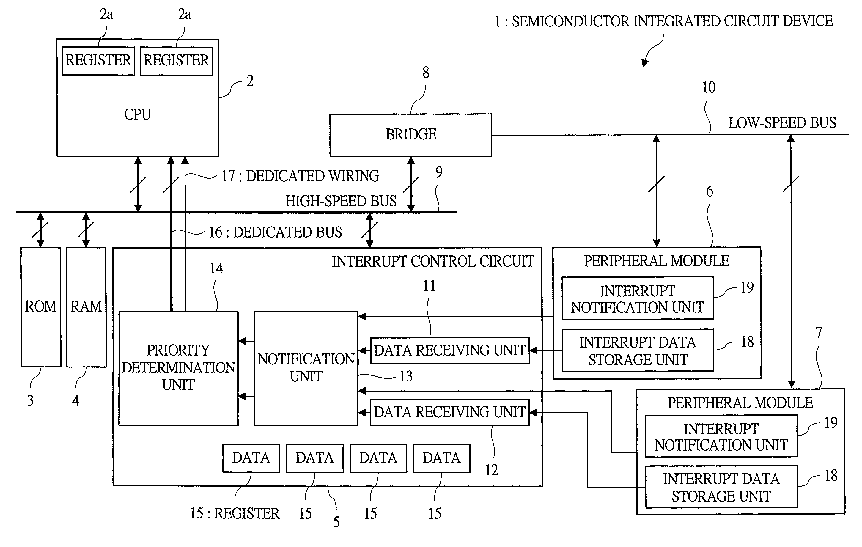
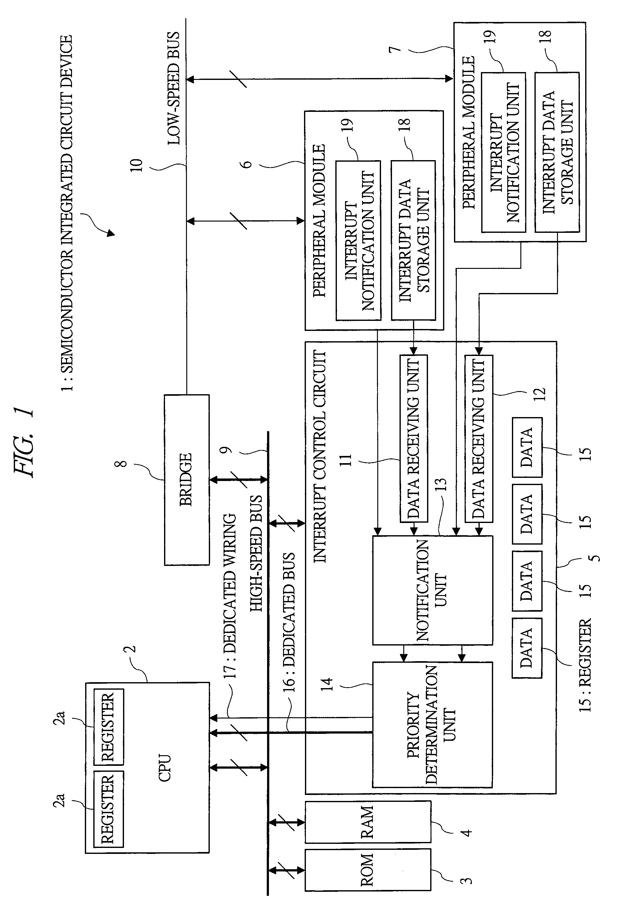
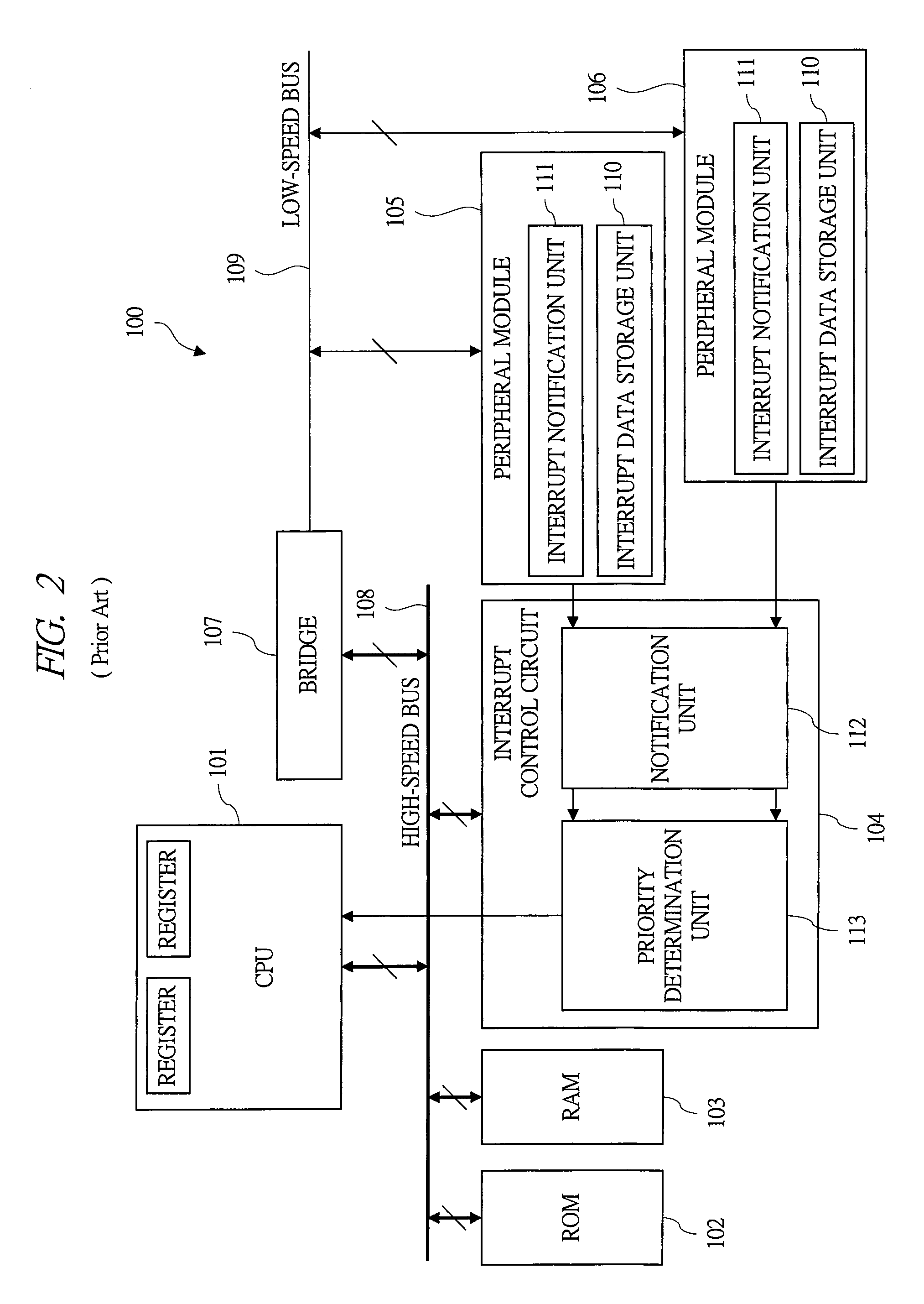
[0041]FIG. 1 is a block diagram showing an example of a semiconductor integrated circuit device according to the first embodiment of the present invention, FIG. 2 is a block diagram showing an example of a general semiconductor integrated circuit device studied by the inventor of the present invention, FIG. 3 is a block diagram showing an example of a semiconductor integrated circuit device described in the Patent Document 1, FIG. 4 is an explanatory diagram showing an example of an interrupt processing of motors, and FIG. 5 is a diagram showing an example of interrupt function programs used in the semiconductor integrated circuit devices shown in FIG. 1 and FIG. 2.

[0042]In the first embodiment, the semiconductor integrated circuit device 1 is mounted in, for example, an in-vehicle ECU (Electric Control Unit). The ECU performs the control of various types of systems such as the information system including a navigation system and an audio system, the power train system including a m...

second embodiment

[0104]FIG. 6 is a block diagram showing an example of a semiconductor integrated circuit device according to the second embodiment of the present invention, FIG. 7 is a timing chart showing an example of the interrupt processing in the semiconductor integrated circuit device of FIG. 6, FIG. 8 is a timing chart showing an example of the interrupt processing in the case where the semiconductor integrated circuit device of FIG. 2 studied by the inventor of the present invention has a dual-core configuration, and FIG. 9 is a timing chart showing an example of the interrupt processing in the case where the semiconductor integrated circuit device of FIG. 3 studied by the inventor of the present invention has a dual-core configuration.

[0105]In the second embodiment, the semiconductor integrated circuit device 1a has a multi-core configuration. This is the difference from the semiconductor integrated circuit device 1 of FIG. 1 in the first embodiment. In the semiconductor integrated circuit...

third embodiment

[0136]The speeding up of the interrupt notification from the peripheral module 6 or the peripheral module 7 to the CPU 2 has been described in the first embodiment. In the third embodiment, the processing after the reception of the interrupt in the CPU 2 will be described.

[0137]In the first embodiment, in response to the interrupt request signal from the peripheral module 6 or the peripheral module 7, the priority determination unit 14 of the interrupt control circuit 5 determines the interrupt to be preferentially notified to the CPU 2 and notifies it to the CPU 2 via the dedicated wiring 17. The CPU 2 accesses the ROM 3 via the high-speed bus 9 based on the interrupt data stored in the register 2a.

[0138]At this point of time, when the other bus master circuit, for example, a DMA transfer control circuit (DMAC) connected to the high-speed bus 9 uses the high-speed bus 9, the determination of the bus use right based on the bus use priority of the CPU 2 and the bus master circuit is...


PUM


Abstract

When an interrupt event occurs, an interrupt request signal and interrupt data are output from an arbitrary peripheral module to an interrupt control circuit. The interrupt control circuit stores the received interrupt data in a register and performs a priority determination of the interrupt request signal. Subsequently, the interrupt control circuit transfers the determination result as an interrupt request signal via a dedicated wiring and the interrupt data of the register via a dedicated bus to the CPU, respectively. Upon reception of the interrupt request, the CPU reads a corresponding interrupt processing function from a ROM and performs the processing of the interrupt data based on the input interrupt request signal.

Description

CROSS-REFERENCE TO RELATED APPLICATION[0001]The present application claims priority from Japanese Patent Application No. 2009-202183 filed on Sep. 2, 2009 and Japanese Patent Application No. 2010-048918 filed on Mar. 5, 2010, the contents of which are hereby incorporated by reference to this application.TECHNICAL FIELD OF THE INVENTION[0002]The present invention relates to an interrupt processing technique in a semiconductor integrated circuit device, and more particularly to a technique effective in reducing a load factor of a central processing unit (CPU) in the interrupt processing.BACKGROUND OF THE INVENTION[0003]With respect to an in-vehicle semiconductor integrated circuit device, for example, it has been widely known that communication between electrical control units (ECU) in each of which the semiconductor integrated circuit device is mounted is performed by using an in-vehicle serial protocol such as a controller area network (CAN).[0004]In that case, particularly in a bod...

Claims


Application Information

Patent Timeline
IPC IPC(8): G06F13/26
CPCG06F13/26Y02D10/00
Inventor FUJII
Owner RENESAS ELECTRONICS CORP
Learn More