GaN SINGLE CRYSTAL SUBSTRATE AND METHOD OF MANUFACTURING THEREOF AND GaN-BASED SEMICONDUCTOR DEVICE AND METHOD OF MANUFACTURING THEREOF

a single crystal substrate and manufacturing method technology, applied in the direction of crystal growth process, polycrystalline material growth, chemically reactive gases, etc., can solve the problems of large blue shift of light emission, difficult to obtain single crystal substrates of a large area, deteriorated luminous efficacy, etc., to achieve superior characteristics, large area, and the effect of large area

Active Publication Date: 2011-03-10
SUMITOMO ELECTRIC IND LTD
View PDF5 Cites 7 Cited by
  • Summary
  • Abstract
  • Description
  • Claims
  • Application Information

AI Technical Summary

Benefits of technology

[0014]An object of the present invention is to solve the above-described problems and provide a GaN single crystal substrate suitable for manufacture of a GaN-based semiconductor device having superior characteristics and a uniform distribution of characteristics, specifically a GaN single crystal substrate having a large area and a main surface whose plane orientation is other than (0001) and (000-1), and having at least one of a substantially uniform distribution of the carrier concentration in the main surface, a substantially uniform distribution of the dislocation density in the main surface, and a small photoelasticity distortion in the main surface that is a distortion measured by photoelasticity, and a method of manufacturing the GaN single crystal substrate. The present invention also has an object of providing a GaN-based semiconductor device having superior characteristics and a uniform distribution of characteristics, and including such a GaN single crystal substrate and at least one GaN-based semiconductor layer formed on the main surface of the substrate, and a method of manufacturing the GaN-based semiconductor device.

Problems solved by technology

Regarding a light emitting device including a substrate of a group III nitride crystal having a main surface whose plane orientation is {0001}, and a light emitting layer of an MQW (multiple quantum well) structure on the main surface, the polarity in the direction of the group III nitride crystal causes spontaneous polarization in the light emitting layer, resulting in a large blue shift of light emission and a deteriorated luminous efficacy.
Even if the manufacturing method disclosed in Japanese Patent Laying-Open No. 2008-143772 (Patent Document 1) is used, the group III nitride crystal grown on the main surface whose plane orientation is {1-100}, {11-20} or {23-50} is partially polycrystallized, resulting in a problem that a single crystal substrate of a large area is difficult to obtain.
A resultant problem is therefore a large variation of the carrier concentration and a large variation of the specific resistance in the main surface of the group III nitride crystal having been grown, and accordingly large variations of characteristics of a semiconductor device for which such a substrate is used.
A resultant problem is therefore a large variation of the dislocation density in the main surface of a grown group III nitride crystal, and thus large variations of characteristics of a semiconductor device using such a substrate.
Furthermore, because of a large variation of the dislocation density in the main surface of the grown group III nitride crystal, a group III nitride crystal substrate made from such a group III nitride crystal has a main surface in which a microscopic variation of distortion is generated, resulting in a problem that a large local distortion is generated.

Method used


Image

  • GaN SINGLE CRYSTAL SUBSTRATE AND METHOD OF MANUFACTURING THEREOF AND GaN-BASED SEMICONDUCTOR DEVICE AND METHOD OF MANUFACTURING THEREOF
  • GaN SINGLE CRYSTAL SUBSTRATE AND METHOD OF MANUFACTURING THEREOF AND GaN-BASED SEMICONDUCTOR DEVICE AND METHOD OF MANUFACTURING THEREOF
  • GaN SINGLE CRYSTAL SUBSTRATE AND METHOD OF MANUFACTURING THEREOF AND GaN-BASED SEMICONDUCTOR DEVICE AND METHOD OF MANUFACTURING THEREOF

Examples


embodiment 1

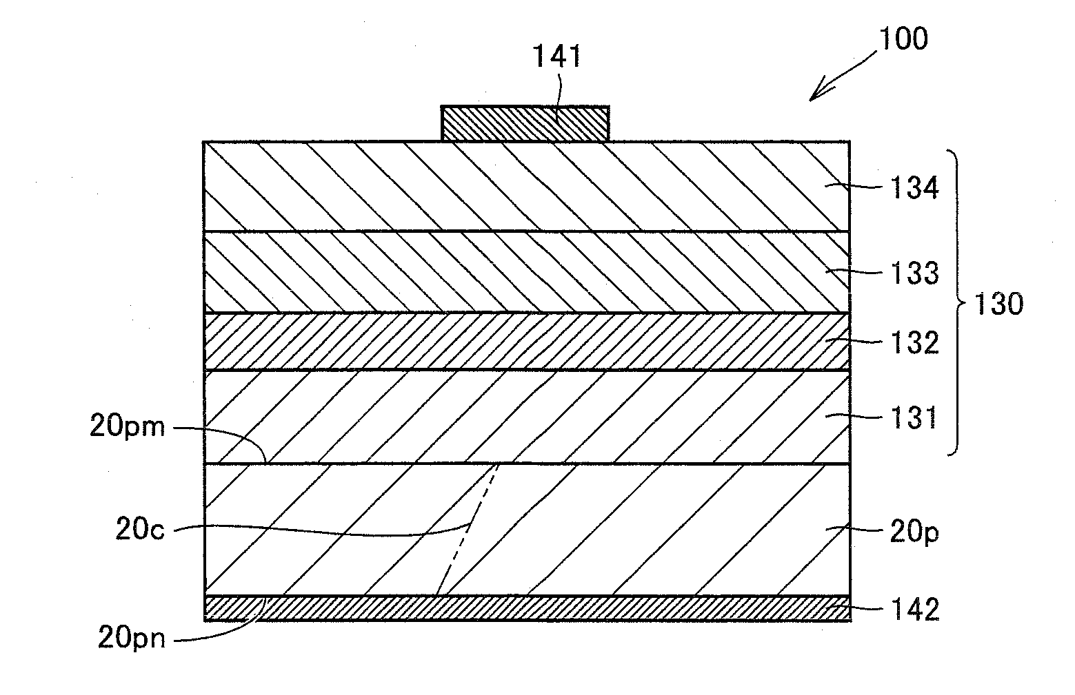
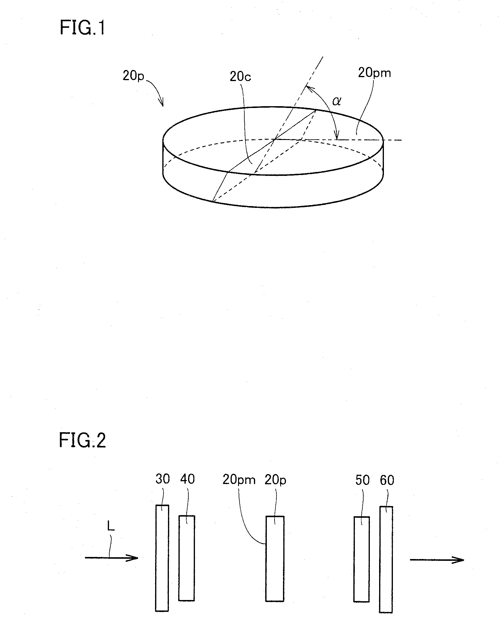
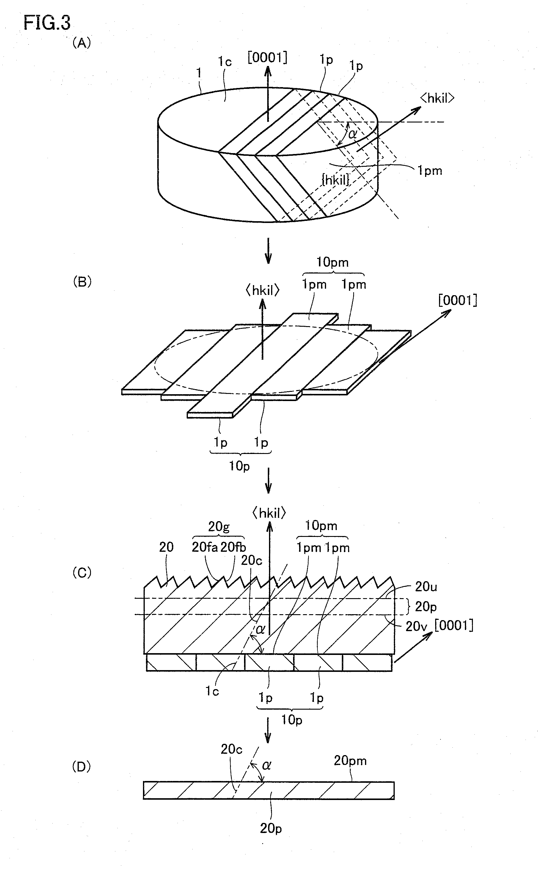
[0035]Referring to FIGS. 1 and 2, a GaN single crystal substrate 20p in an embodiment of the present invention includes a main surface 20pm having an area of not less than 10 cm2. The plane orientation of main surface 20pm is inclined by not less than 65° and not more than 85° with respect to a plane 20c that is one of a (0001) plane and a (000-1) plane. The substrate has at least one of a substantially uniform distribution of the carrier concentration in main surface 20pm, a substantially uniform distribution of the dislocation density in main surface 20pm, and a photoelasticity distortion value of not more than 5×10⁻⁵ where the photoelasticity distortion value is measured by photoelasticity at an arbitrary point in main surface 20pm when light L is applied perpendicularly to main surface 20pm at an ambient temperature of 25° C. GaN single crystal substrate 20p in the present embodiment is suitably used for manufacture of a GaN-based semiconductor device having superior characteris...

embodiment 1a

[0036]Referring to FIG. 1, as to GaN single crystal substrate 20p in the present embodiment, the area of main surface 20pm is not less than 10 cm2, the plane orientation of main surface 20pm is inclined by not less than 65° and not more than 85° with respect to plane 20c that is one of a (0001) plane and a (000-1) plane, and the distribution of the carrier concentration in main surface 20pm is substantially uniform.

[0037]GaN single crystal substrate 20p in the present embodiment has a large area of main surface 20pm of 10 cm2 or more. Further, the plane orientation of main surface 20pm is inclined by an inclination angle α of not less than 65° and not more than 85° with respect to plane 20c that is one of a (0001) plane and a (000-1) plane, and therefore, blue shift of light emission from a GaN-based semiconductor device using such a GaN single crystal substrate 20p is suppressed and degradation in luminous efficacy is thus suppressed. In view of this, the plane orientation of main ...

embodiment 1b

[0042]Referring to FIG. 1, as to GaN single crystal substrate 20p in the present embodiment, the area of main surface 20pm is not less than 10 cm2, the plane orientation of main surface 20pm is inclined by not less than 65° and not more than 85° with respect to plane 20c that is one of a (0001) plane and a (000-1) plane, and the distribution of the dislocation density in main surface 20pm is substantially uniform.

[0043]GaN single crystal substrate 20p in the present embodiment has a large area of main surface 20pm of 10 cm2 or more. Further, the plane orientation of main surface 20pm is inclined by an inclination angle α of not less than 65° and not more than 85° with respect to plane 20c that is one of a (0001) plane and a (000-1) plane, and therefore, blue shift of light emission from a GaN-based semiconductor device using such a GaN single crystal substrate 20p is suppressed and degradation in luminous efficacy is thus suppressed. In view of this, the plane orientation of main su...


PUM

PropertyMeasurementUnit
temperatureaaaaaaaaaa
areaaaaaaaaaaa
off angleaaaaaaaaaa

Abstract

A GaN single crystal substrate has a main surface with an area of not less than 10 cm2, the main surface has a plane orientation inclined by not less than 65° and not more than 85° with respect to one of a (0001) plane and a (000-1) plane, and the substrate has at least one of a substantially uniform distribution of a carrier concentration in the main surface, a substantially uniform distribution of a dislocation density in the main surface, and a photoelasticity distortion value of not more than 5×10⁻⁵, the photoelasticity distortion value being measured by photoelasticity at an arbitrary point in the main surface when light is applied perpendicularly to the main surface at an ambient temperature of 25° C. Thus, the GaN single crystal substrate suitable for manufacture of a GaN-based semiconductor device having a small variation of characteristics can be obtained.

Description

BACKGROUND OF THE INVENTION[0001]1. Field of the Invention[0002]The present invention relates to a GaN single crystal substrate suitable for manufacture of a GaN-based semiconductor device having characteristics with small variations, specifically to a GaN single crystal substrate having a large area and a main surface whose plane orientation is other than (0001) and (000-1) (namely other than {0001}), and having at least one of a substantially uniform distribution of the carrier concentration in the main surface, a substantially uniform distribution of the dislocation density in the main surface, and a small photoelasticity distortion in the main surface that is a distortion measured by photo elasticity, and relates to a method of manufacturing the GaN single crystal substrate. The invention also relates to a GaN-based semiconductor device including such a GaN single crystal substrate and at least one GaN-based semiconductor layer formed on the main surface of the substrate, and a ...

Claims


Application Information

Patent Timeline
Patent Type & Authority Applications(United States)
IPC IPC(8): H01L29/20C30B25/18H01L21/20
CPCC30B25/20C30B29/406H01L21/02389H01L21/02433H01L29/36H01L29/2003H01L33/0075H01L33/16H01L21/0254
Inventor FUJIWARA, SHINSUKEUEMATSU, KOJIOSADA, HIDEKINAKAHATA, SEIJI
Owner SUMITOMO ELECTRIC IND LTD
Why Eureka
Try Eureka