Semiconductor device and method for manufacturing the same

a technology of semiconductor devices and semiconductors, applied in the direction of semiconductor devices, basic electric elements, electrical equipment, etc., can solve the problems of transistor operation errors and device characteristics reduction, and achieve the effect of improving device characteristics

Inactive Publication Date: 2011-03-10
SAMSUNG ELECTRO MECHANICS CO LTD
View PDF5 Cites 81 Cited by
  • Summary
  • Abstract
  • Description
  • Claims
  • Application Information

AI Technical Summary

Benefits of technology

[0007]The present invention has been proposed in order to overcome the above-described problems and it is, therefore, an object of the present invention to provide a semiconductor device which has an HEMT structure for improving device's characteristics, and a method for manufacturing the same.

Problems solved by technology

However, the N-FET having the same structure has problems in that an electric field is concentrated on the gate and drain electrodes, and thus errors occur in transistor operation.
In particular, since the semiconductor device with the HEMT structure is required to be operated at a high voltage, a high electric field concentrated on the gate and drain electrodes causes a reduction in device's characteristics.

Method used


Image

  • Semiconductor device and method for manufacturing the same
  • Semiconductor device and method for manufacturing the same
  • Semiconductor device and method for manufacturing the same

Examples


Embodiment Construction

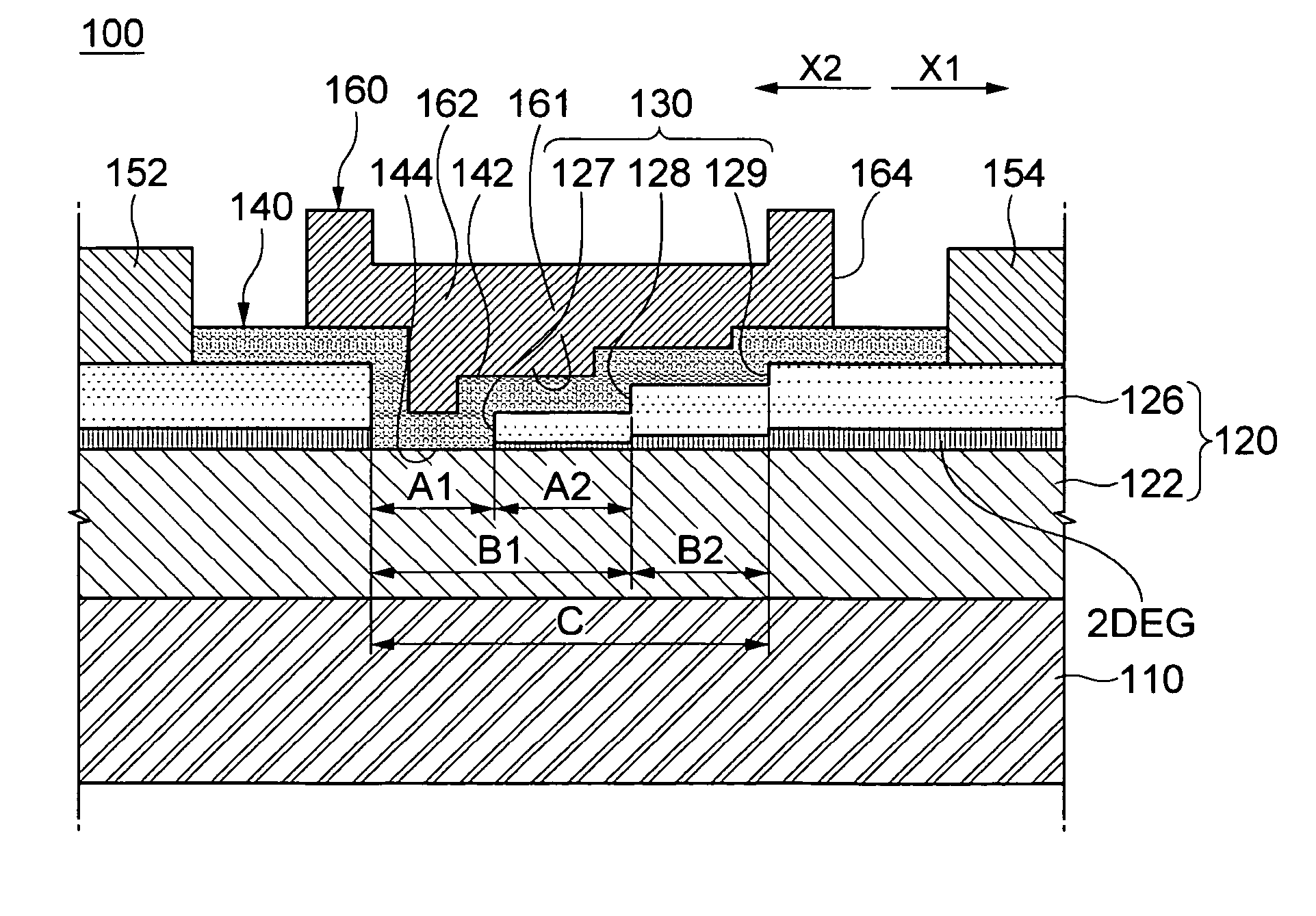
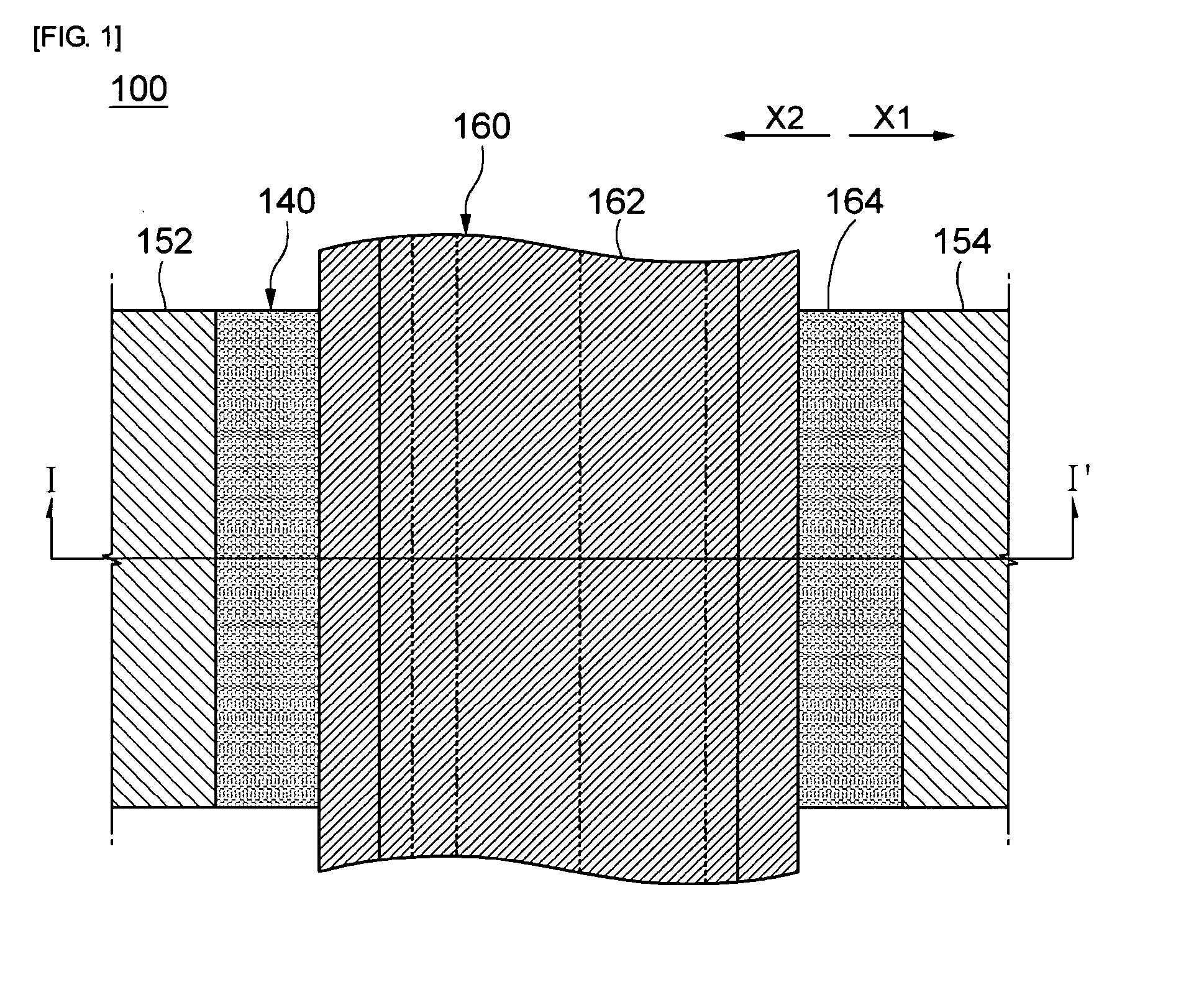
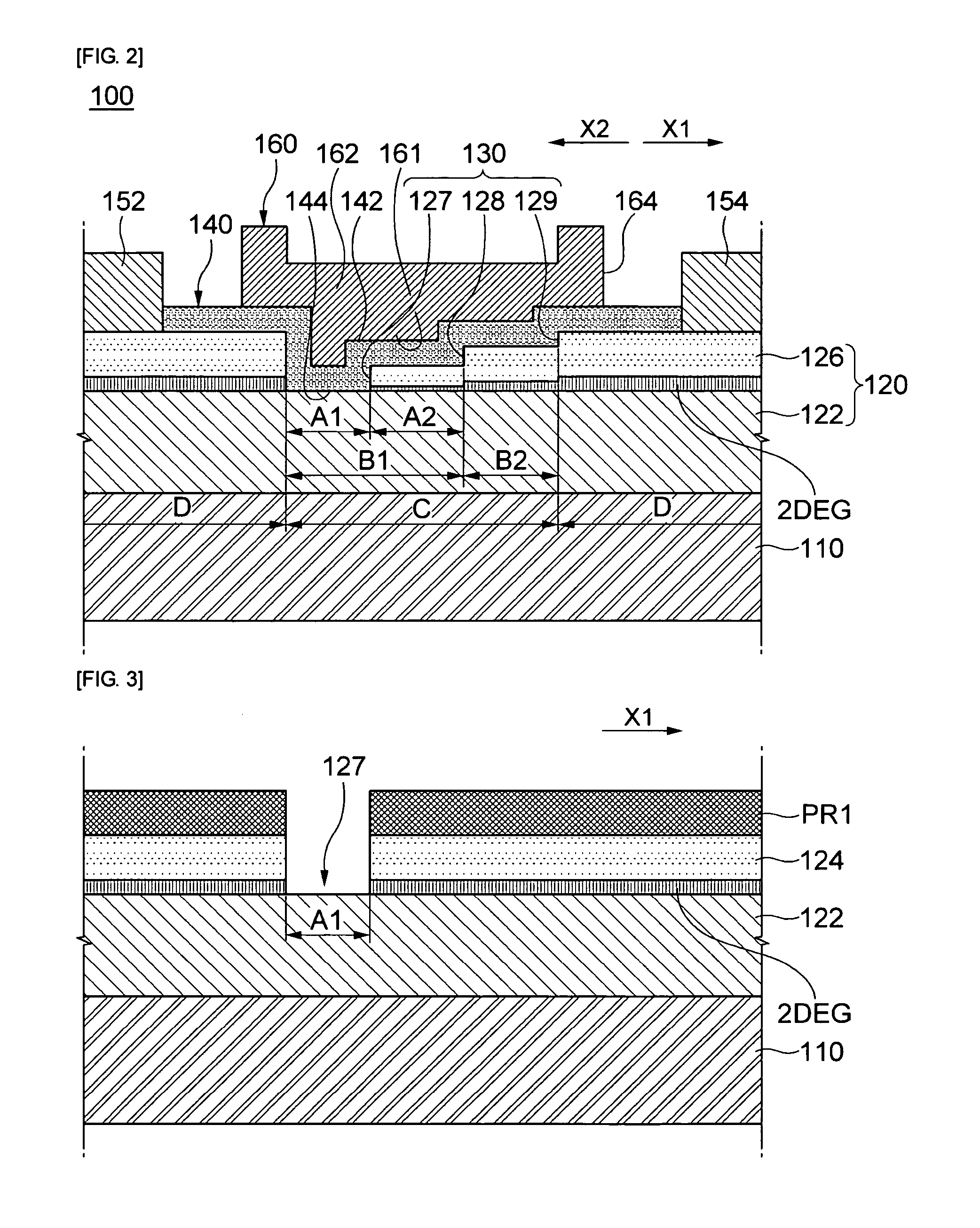
[0028]The invention now will be described more fully hereinafter with reference to the accompanying drawings, in which exemplary embodiments of the invention are shown. This invention may, however, be embodied in many different forms and should not be construed as limited to the embodiments set forth herein. Rather, these embodiments are provided so that this disclosure will be thorough and complete, and will fully convey the scope of the invention to those skilled in the art. Like reference numerals refer to like elements throughout.

[0029]The terminology used herein is for the purpose of describing particular embodiments only and is not intended to be limiting of example embodiments. As used herein, the singular forms “a,”“an” and “the” are intended to include the plural forms as well, unless the context clearly indicates otherwise. It will be further understood that the terms “comprises” and / or “comprising,” when used in this specification, specify the presence of stated features,...


PUM


Abstract

The present invention provides a semiconductor device including: a base substrate; a semiconductor layer which is disposed on the base substrate and has a recess structure formed thereon; a gate structure covering the recess structure; a source electrode and a drain electrode which are disposed to be spaced apart from each other with respect to the gate structure interposed therebetween, on the semiconductor layer, wherein the semiconductor layer having an upper layer whose thickness is increased toward a first direction facing the drain electrode from the gate structure.

Description

CROSS-REFERENCE TO RELATED APPLICATIONS[0001]This application claims the benefit of Korean Patent Application No. 10-2009-0084593 field with the Korea Intellectual Property Office on Sep. 8, 2009, the disclosure of which is incorporated herein by reference.BACKGROUND OF THE INVENTION[0002]1. Field of the Invention[0003]The present invention relates to a semiconductor device; and, more particularly, to a semiconductor device with an N-FET structure, and a method for manufacturing the same.[0004]2. Description of the Related Art[0005]In general, III-nitride-based semiconductor which includes III-elements such as Ga, Al, In, and so on, and N is characterized by a wide energy band gap, high electron mobility and saturation electron speed, and high thermal-chemical stability. Such an Nitride-based Field Effect Transistor (N-FET) is manufactured based on a semiconductor material with a wide energy band gap, e.g., materials of GaN, AlGaN, InGaN, and AlINGaN.[0006]A typical N-FET has a High...

Claims


Application Information

Patent Timeline
Patent Type & Authority Applications(United States)
IPC IPC(8): H01L29/78H01L21/336
CPCH01L29/0657H01L29/2003H01L29/7787H01L29/66462H01L29/4236H01L29/42376
Inventor PARK, KI YEOLLEE, JUNG HEEHA, JONG BONGPARK, YOUNG HWANJEON, WOO CHUL
Owner SAMSUNG ELECTRO MECHANICS CO LTD
Why Eureka
Try Eureka