Circuit module and method of manufacturing the same

Active Publication Date: 2011-03-17
IMBERATEK LLC
View PDF5 Cites 18 Cited by
  • Summary
  • Abstract
  • Description
  • Claims
  • Application Information

AI Technical Summary

Benefits of technology

[0020]The possibility to use contact elements that are narrower than the contact area can, for its part, provide advantages, for example, by allowing the conductors connected to the contact elements to also be made narrow, especially in embodiments, in which the contact element is essentially of even width vertically, or only narrows moderately towards the component.
[0021]In an embodiment of the manufacturing process, in which contact openings are made in the conductor foil of the conductor-pattern layer prior to attaching the component, the compone

Problems solved by technology

The practicability of the manufacturing method is also affected by the availability of raw materials and the ability of the method to place different types of component in a circuit module.
However, at present copper is quite little used as a conductor material in semiconductor processes.
Copper conductors of a circuit module can be grown directly on top of aluminium contact areas, but the contact between copper and aluminium is brittle, so that a module of this kind is not optimal i

Method used


Image

  • Circuit module and method of manufacturing the same
  • Circuit module and method of manufacturing the same
  • Circuit module and method of manufacturing the same

Examples


fourth embodiment

rmediate stage of a circuit module when using a manufacturing method according to a

[0029]FIG. 25 shows one possible example of a contact hole and its dimensions made for a contact element of a circuit module.

[0030]FIG. 26 shows examples of possible contact holes.

[0031]FIG. 27 shows some embodiments of intermediate layers manufactured in the contact hole of FIG. 26.

[0032]FIG. 28 shows one contact-element structure.

[0033]FIG. 29 shows a second contact-element structure.

[0034]FIG. 30 shows a third contact-element structure.

[0035]FIG. 31 shows a fourth contact-element structure.

[0036]FIG. 32 shows a fifth contact-element structure.

[0037]FIG. 33 shows a sixth contact-element structure.

MODES FOR CARRYING OUT THE INVENTION

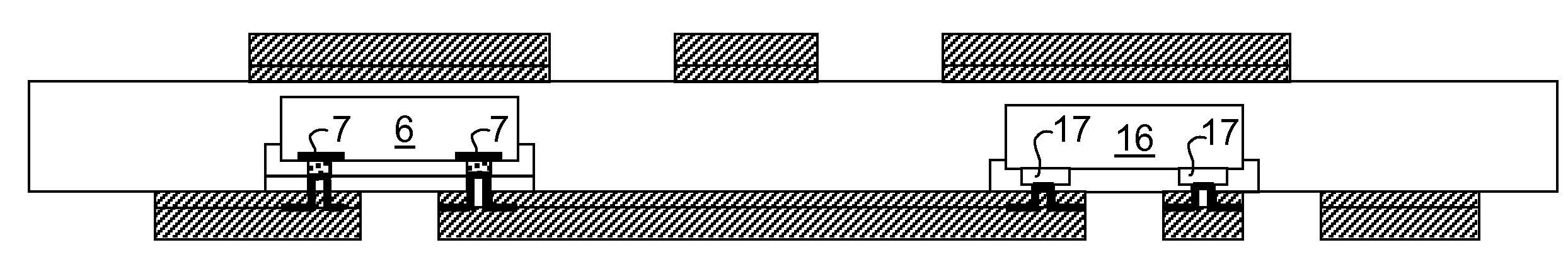
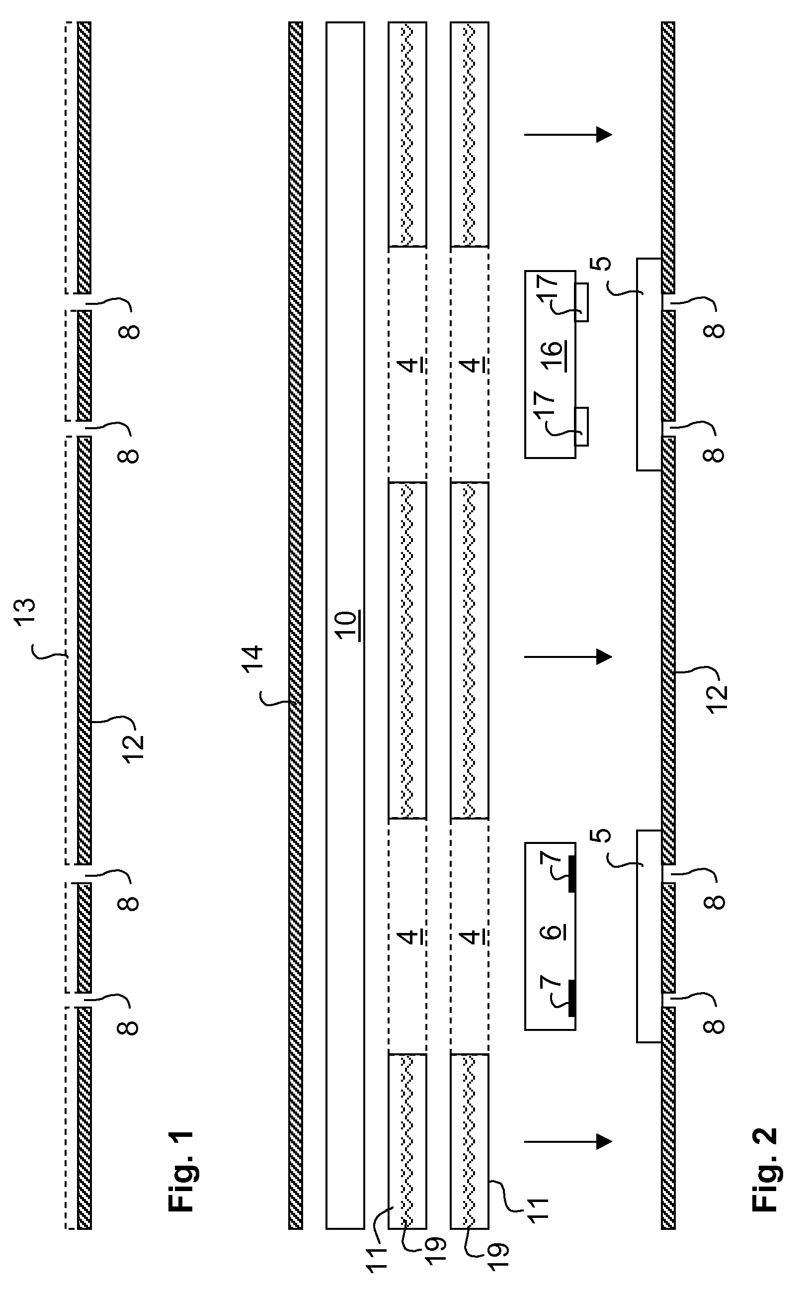
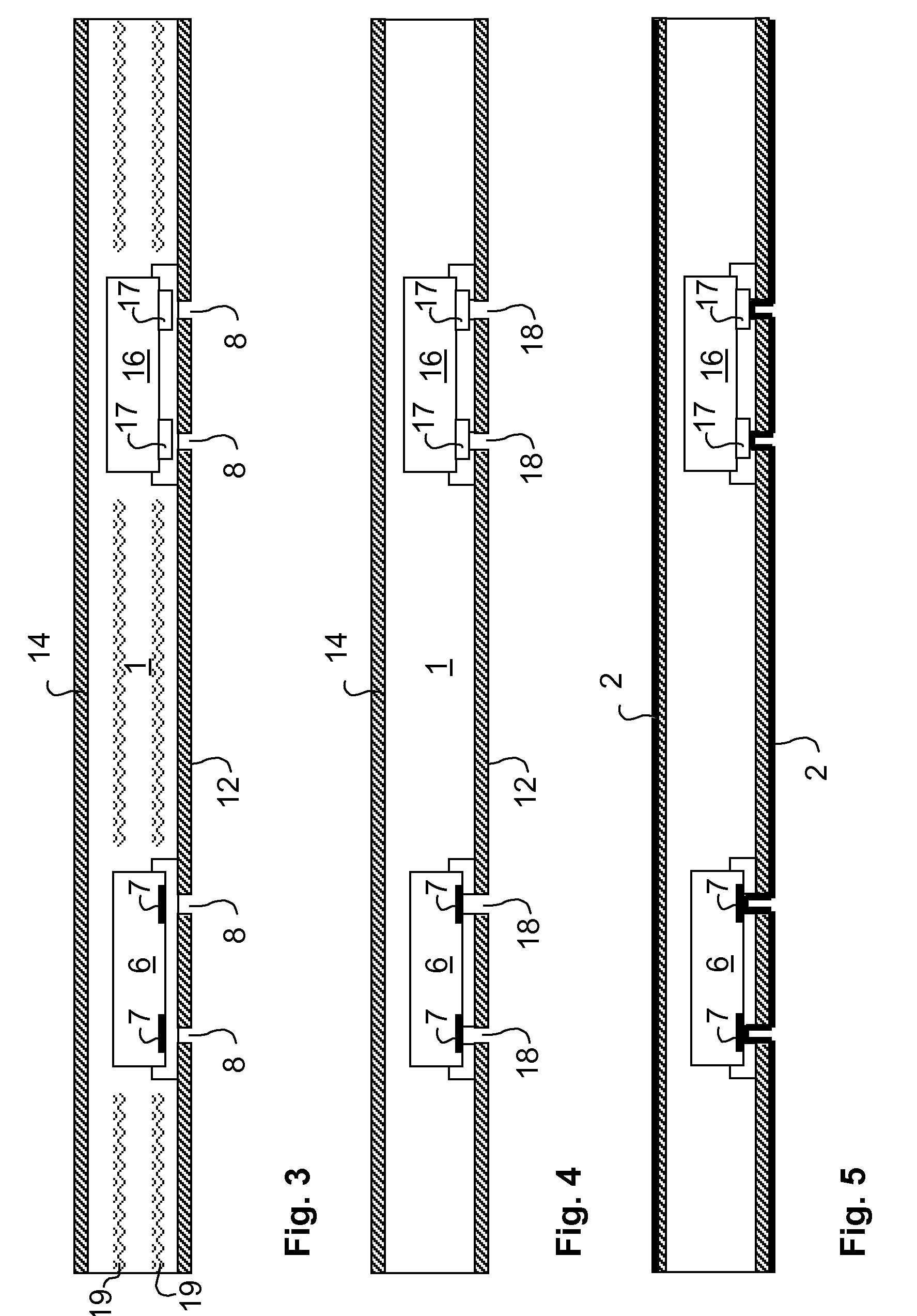
[0038]FIGS. 1-9 show one exemplary application of the manufacturing method according to one embodiment. In this embodiment, manufacture begins from a conductor foil 12, which of metal, for example. A suitable conductor foil 12 is, for example, a copper film, the thickness...


PUM

PropertyMeasurementUnit
Timeaaaaaaaaaa
Fractionaaaaaaaaaa
Widthaaaaaaaaaa

Abstract

Manufacturing method and circuit module, which comprises an insulator layer (1) and, inside the insulator layer (1), at least one component (6), which comprises contact areas (7), the material of which contains a first metal. On the surface of the insulator layer (1) are conductors (22), which comprise at least a first layer (12) and a second layer (32), in such a way that at least the second layer (32) contains a second metal. The circuit module comprises contact elements between the contact areas (7) and the conductors (22) for forming electrical contacts. The contact elements, for their part, comprise, on the surface of the material of the contact area (7), an intermediate layer (2), which contains a third metal, in such a way that the first, second, and third metals are different metals and the contact surface area (ACONT 1), between the intermediate layer (2) and the contact area (7) is less that the surface area (APAD) of the contact area (7).

Description

TECHNICAL FIELD[0001]The present invention relates to circuit modules, which comprise an insulator layer and, inside the insulator layer, at least one component, which comprises contact areas. In addition, the circuit modules comprise conductors on the surface of the insulator layer, through which a component can be connected to become part of a circuit outside the component. For creating electrical contacts, the circuit modules comprise contact elements between the contact areas of the component and the conductors.[0002]The invention also relates to methods for manufacturing the aforementioned circuit modules.BACKGROUND ART[0003]In the background art, several different ways are described, by means of which circuit modules containing components located inside an insulator material can be manufactured. The background art also discloses several solutions for manufacturing electrical contacts to the contact terminals of a component, by means of contact elements, and methods for manufac...

Claims


Application Information

Patent Timeline
IPC IPC(8): H05K1/09H05K1/16H05K1/00H01R43/00
CPCH01L21/486Y10T29/4913H01L23/5389H01L24/24H01L24/82H01L2221/68359H01L2224/13144H01L2224/13147H01L2224/24227H01L2924/01005H01L2924/01013H01L2924/0102H01L2924/01027H01L2924/01029H01L2924/0103H01L2924/01033H01L2924/01074H01L2924/01075H01L2924/01078H01L2924/01079H01L2924/01082H01L2924/14H01L2924/1433H01L2924/15153H01L2924/1517H05K1/188H05K3/305H05K2201/0355H05K2201/09509H05K2201/0969H05K2201/10674H05K2203/063H01L23/5384Y10T29/49117H01L2924/1461H01L2924/12041H01L2224/0401H01L2224/24137H01L2224/92144H01L2224/12105H01L24/19H01L2924/01006H01L2924/01023H01L2924/01024H01L2924/01047H01L23/49866H01L2224/04105H01L2924/00H01L2224/32245H01L2924/12042H01L2924/351H05K1/185H01L23/498H01L23/49811H01L23/49838H05K1/09H05K1/182
Inventor PALM, PETTERITUOMINEN, RISTOIIHOLA, ANTTI
Owner IMBERATEK LLC
Why Eureka
Try Eureka