
Wafer-level lens array, method of manufacturing wafer-level lens array, lens module and imaging unit

a technology of wafer-level lenses and lens modules, which is applied in the field of wafer-level lens arrays, can solve the problems of large deformation of the lens surface, large deformation of the lens unit, and large deformation of the resin, so as to prevent the positional deviation, prevent the deterioration of image quality, and design easy

Inactive Publication Date: 2011-03-17
FUJIFILM CORP
View PDF10 Cites 15 Cited by
  • Summary
  • Abstract
  • Description
  • Claims
  • Application Information

AI Technical Summary

Benefits of technology

[0021]An object of the invention is to provide a wafer-level lens array, a method of manufacturing a wafer-level lens array, a lens module, and an imaging unit that can prevent the influence of, for example, the shrinkage of a forming material, prevent the positional deviation between lenses when the wafer-level lens arrays overlap each other or when the wafer-level lens array overlaps an imaging element array, and be easily designed.
[0023]In the manufacturing method, the substrate unit and a plurality of lens units are formed by different processes and are made of materials that substantially the same optical characteristics. Since the substrate unit and the plurality of lens units are formed by different processes, the lens units are not affected by shrinkage due to curing when the substrate unit is formed. Since the lens units are formed on the substrate unit, it is possible to prevent the positional deviation between the lens units.
[0025]According to the above-mentioned embodiment of the invention, since the substrate unit is formed beforehand, shrinkage due to curing does not occur in the substrate unit when the lens units are formed. Therefore, when a liquid resin on the substrate is deformed into a desired shape by the mold and is then cured, the resin is cured while being adhered to the surface of the substrate unit, and the amount of shrinkage of a portion of the resin that comes into contact with the substrate unit in a direction along the surface of the substrate unit is significantly less than the amount of shrinkage when the entire substrate unit is cured and shrunken at the same time. Therefore, it is possible to reduce the shrinkage of the lens unit in the diametric direction and form a high-quality lens unit, as compared to the structure in which the substrate unit is formed at the same time. When the wafer-level lens arrays overlap each other or when the wafer-level lens array overlaps the imaging element array, it is possible to provide a wafer-level lens array, a method of manufacturing a wafer-level lens array, a lens module, and an imaging unit that can prevent the positional deviation between the lenses and be easily designed.

Problems solved by technology

When the resin is cured by light or heat and is shrunken, there is a concern that the lens unit will be shrunken in the diametric direction, and the shape of the lens surface will be greatly deformed.
In addition, the resin is not uniformly shrunken, or expanded or contracted in the entire wafer.
Therefore, when the wafer-level lens arrays overlap each other or when the wafer-level lens array overlaps the imaging element array, there is a concern that the positional deviation between the lens units will occur due to shrinkage, or contraction or expansion.
As a result, the design becomes complicated.
When the lens is used as an imaging lens, image quality deteriorates due to, for example, flare caused by the reflection of light from the interface.

Method used


Image

  • Wafer-level lens array, method of manufacturing wafer-level lens array, lens module and imaging unit
  • Wafer-level lens array, method of manufacturing wafer-level lens array, lens module and imaging unit
  • Wafer-level lens array, method of manufacturing wafer-level lens array, lens module and imaging unit

Examples


Embodiment Construction

[0045]First, the structure of a wafer-level lens array, a lens module, and an imaging unit according to an embodiment of the invention will be described.

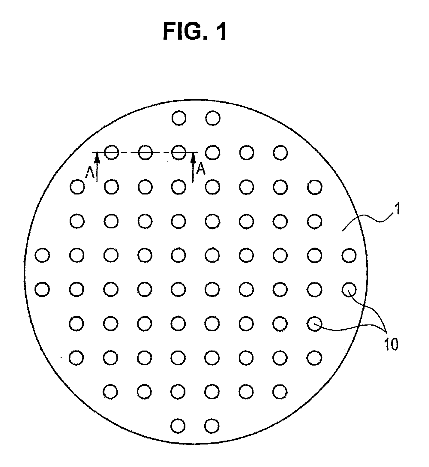
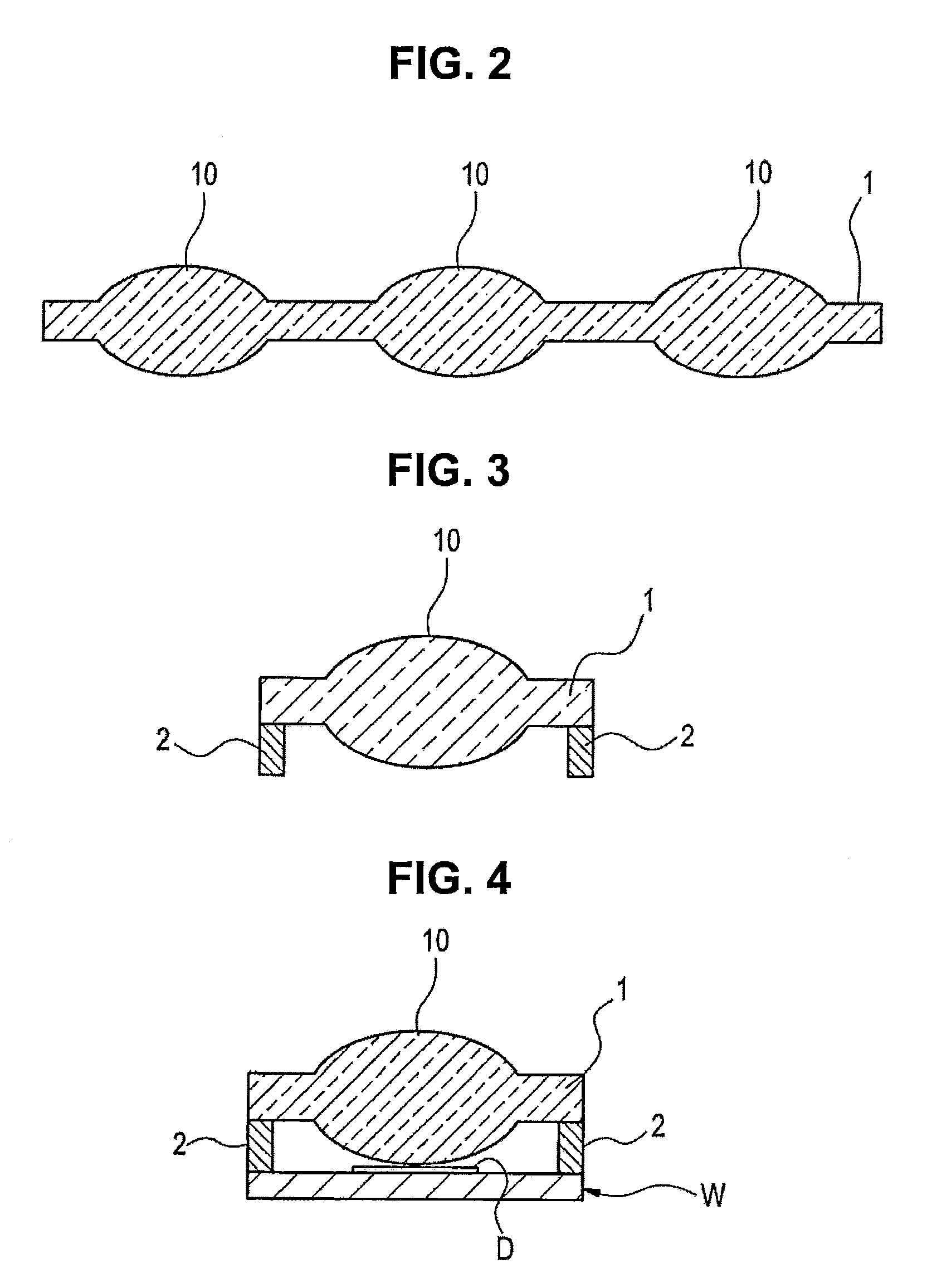
[0046]FIG. 1 is a plan view illustrating an example of the structure of the wafer-level lens array. FIG. 2 is a cross-sectional view illustrating the wafer-level lens array taken along the line A-A of FIG. 1.

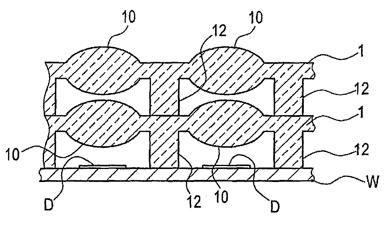
[0047]The wafer-level lens array includes a substrate unit 1 and a plurality of lens units 10 that is arranged on the substrate unit 1. The plurality of lens units 10 is one-dimensionally or two-dimensionally arranged on the substrate unit 1. In this embodiment, as shown in FIG. 1, an example of the structure in which the plurality of lens units 10 is two-dimensionally arranged on the substrate unit 1 will be described. The lens units 10 are made of a resin that has substantially the same optical characteristics as that forming the substrate unit 1 and are formed integrally with the substrate unit 1. The shape of the lens unit 1...


PUM


Abstract

Disclosed are a wafer-level lens array, a method of manufacturing a wafer-level lens array, a lens module, and an imaging unit that can prevent the influence of, for example, the shrinkage of a forming material, prevent the positional deviation between lenses when the wafer-level lens arrays overlap each other or when the wafer-level lens array overlaps an imaging element array, and be easily designed.A method of manufacturing a wafer-level lens array including a substrate unit and a plurality of lens units that is arranged on the substrate unit includes: forming the substrate unit; and integrally forming the lens units that are made of a resin having substantially the same optical characteristics as a material forming the substrate unit with the substrate unit.

Description

CROSS-REFERENCE TO RELATED APPLICATIONS[0001]This application is based upon and claims the benefit of priority from the Japanese Patent Application No. 2009-211853 filed on Sep. 14, 2009; the entire contents of which are incorporated herein by reference.BACKGROUND OF THE INVENTION[0002]1. Field of the Invention[0003]The present invention relates to a wafer-level lens array, a method of manufacturing a wafer-level lens array, a lens module and an imaging unit.[0004]2. Description of the Related Art[0005]In recent years, portable terminals of electronic apparatuses, such as mobile phones or PDAs (Personal Digital Assistants), include small and thin imaging units. In general, the imaging unit includes a solid-state imaging element, such as a CCD (Charge Coupled Device) image sensor or a CMOS (Complementary Metal-Oxide Semiconductor) image sensor, and a lens for forming an object image on the solid-state imaging element.[0006]With a reduction in the size and thickness of the portable te...

Claims


Application Information

Patent Timeline
IPC IPC(8): H04N5/335G02B7/02B29D11/00
CPCG02B13/0085B29D11/00307
Inventor YAMADA, DAISUKEMATSUNO, RYO
Owner FUJIFILM CORP
Learn More