Method for producing a printed circuit board and use and printed circuit board

a technology of printed circuit board and tensile strength, applied in the direction of application, show cabinet, soldering media, etc., can solve the problems of insufficient tensile strength of wire-bond connection, and high cost, so as to improve the tensile strength or enhanced tensile strength exhibiting, the effect of improving the adhesion of individual components

Inactive Publication Date: 2011-03-24
AT & S AUSTRIA TECH & SYSTTECHN AKTIENGES
View PDF6 Cites 11 Cited by
  • Summary
  • Abstract
  • Description
  • Claims
  • Application Information

AI Technical Summary

Benefits of technology

[0007]Departing from a method of the initially defined kind, the present invention, therefore, aims to avoid the above-mentioned drawbacks in respect to the problems of maintaining a proper bonding and fixation of a component to or in a printed circuit board and/or connection of individual elements of a printed circuit board, and, in p

Problems solved by technology

Besides the high costs involved in such a bonding process, the main disadvantages reside in the sequential succession of the production of individual connections such that no parallel process can be performed and, in particular, every contact or every region to be contacted must be separately produced, thus overall resulting in an expensive method.
Due to the types of metal wire used, a partially high thermal load will, moreover, be exerted on the components or elements to be connected or bonded at temperatures of, for instance, up to about 300° C

Method used


Image

  • Method for producing a printed circuit board and use and printed circuit board
  • Method for producing a printed circuit board and use and printed circuit board
  • Method for producing a printed circuit board and use and printed circuit board

Examples


Embodiment Construction

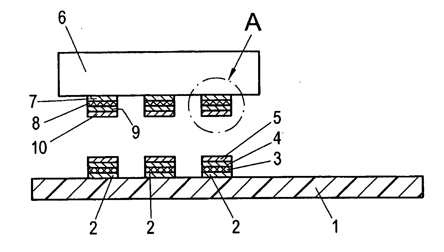
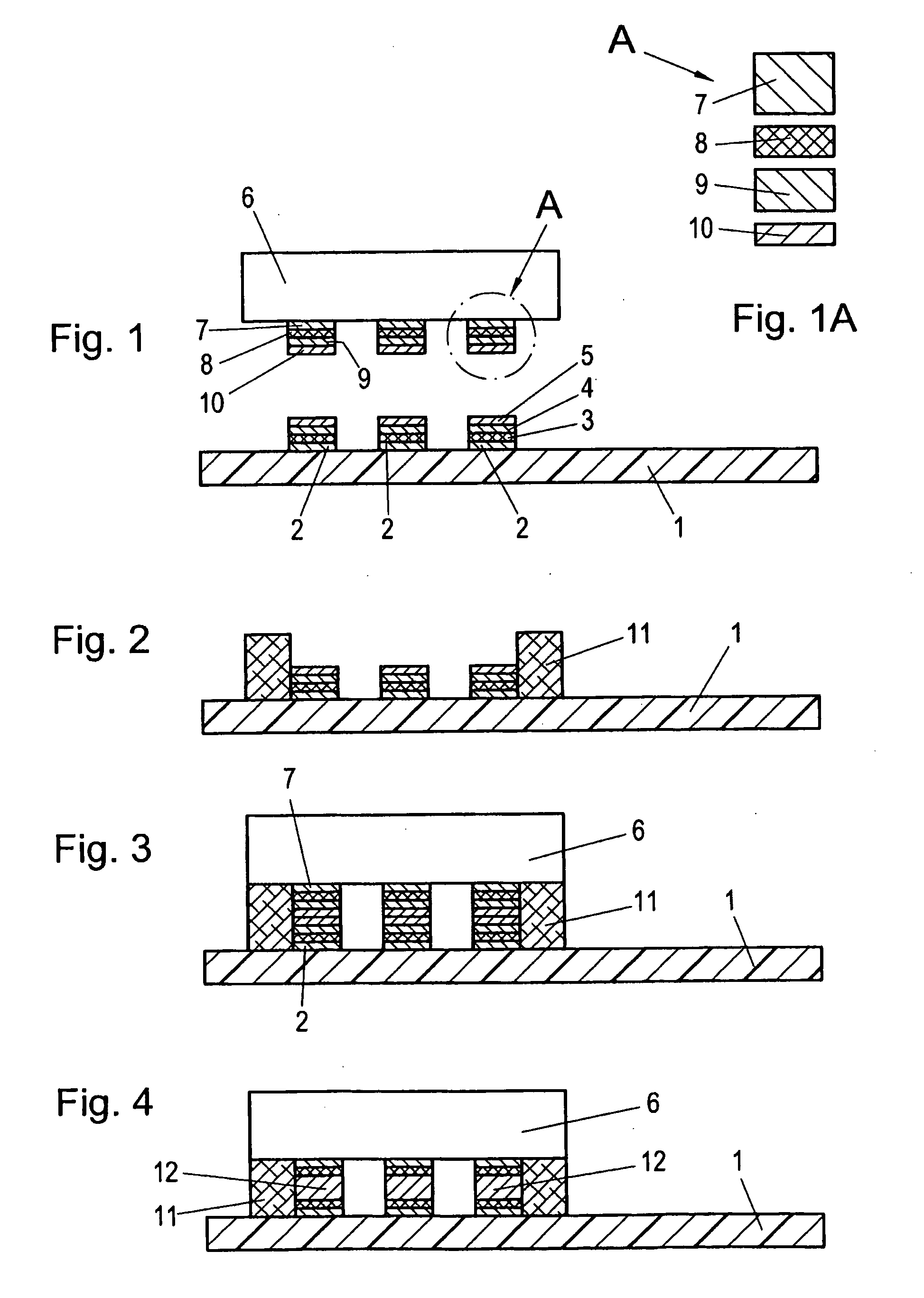
[0030]FIGS. 1 to 4 depict different method steps in the performance of the method for fixing a component to or in a printed circuit board.

[0031]In FIG. 1 it is shown that, on a printed circuit board generally denoted by 1, in the region of contact pads each denoted by 2 and, for instance, made of copper, a barrier layer 3 is arranged on this copper layer 2, on which barrier layer two layers 4 and 5 of different solder materials are subsequently arranged or applied.

[0032]In a similar manner, a barrier layer 8 is each arranged or applied on an electronic component 6 to be connected with the printed circuit board 1 in the region of contact sites or pads 7, on which solder layers 9 and 10 of different materials are again subsequently applied or provided.

[0033]FIG. 1A depicts the subregion A of the component 6 according to FIG. 1 on an enlarged scale, wherein it is apparent that, on the contact layer 7, which is illustrated with an exaggerated thickness, a barrier layer 8 is subsequently...


PUM

PropertyMeasurementUnit
Temperatureaaaaaaaaaa

Abstract

The invention relates to a method for fixing a component (6) to or in a printed circuit board (1) and/or for connecting individual elements of a printed circuit board, wherein regions of a component (6) and/or of a printed circuit board (1) to be interconnected or to be fixed to one another are provided with at least one respective solder layer (4, 5, 9, 10), the solder layers (4, 5, 9, 10) are contacted with each other and are interconnected at a pressure and a temperature that is elevated above ambient conditions, an intermetallic diffusion layer (12) being formed, thereby achieving a high-strength connection. The invention further relates to the use of said method and to a printed circuit board (1).

Description

[0001]This is a national stage of PCT / AT2009 / 000210 filed May 20, 2009 and published in German, which has a priority of Austria no. GM 293 / 2008 filed May 21, 2008, hereby incorporated by reference.FIELD OF THE INVENTION[0002]The present invention relates to a method for fixing a component to or in a printed circuit board and / or for connecting individual elements of a printed circuit board as well as the use of such a method and a printed circuit board.PRIOR ART[0003]In the context of the production of a printed circuit board and, in particular, the fixation of components to or in a printed circuit board and / or the connection of individual elements of a printed circuit board, for instance in the production of a rigid-flexible printed circuit board, three methods are, above all, applied according to the current prior art, in which context reference is, in particular, made to wire-bonding, soldering and bonding by electrically conducting or conductive adhesive films or adhesives. For t...

Claims


Application Information

Patent Timeline
IPC IPC(8): H05K1/09H05K3/30
CPCA47F3/001Y10T29/4913B23K35/0238B23K35/262B23K35/264B23K35/3006B23K35/3013B23K35/302B23K35/3033B23K35/3053B23K2201/36H05K3/244H05K3/328H05K3/3463H05K3/363H05K2203/0278A47F11/10B23K2101/36
Inventor WEICHSLBERGER, GUNTHERSTAHR, JOHANNES
Owner AT & S AUSTRIA TECH & SYSTTECHN AKTIENGES
Why Eureka
Try Eureka