Method for bonding gas barrier film and electronic device, and electronic device and method for producing same

a technology of gas barrier film and electronic device, which is applied in the direction of discharge tube luminescnet screen, final product manufacturing, sustainable manufacturing/processing, etc., can solve the problems of unsatisfactory production efficiency and superfluous step that is still complicated, and achieve high production efficiency

Inactive Publication Date: 2011-03-24
FUJIFILM CORP
View PDF4 Cites 9 Cited by
  • Summary
  • Abstract
  • Description
  • Claims
  • Application Information

AI Technical Summary

Benefits of technology

[0027]The method for bonding a gas barrier film and an electronic device of the invention is simple and attains high production efficiency, not damaging the gas barrier film being fed continuously to the processing system. The method for producing an assembly of a plural number of electronic devices of the invention does not require fitting of a

Problems solved by technology

As a result, the inventors have known that it is difficult to peel the gas barrier film bonding to a wire lead-out part later in the subsequent step

Method used


Image

  • Method for bonding gas barrier film and electronic device, and electronic device and method for producing same
  • Method for bonding gas barrier film and electronic device, and electronic device and method for producing same
  • Method for bonding gas barrier film and electronic device, and electronic device and method for producing same

Examples


production example 1

Formation of Gas Barrier Film

[0084]According to the description in the paragraphs [0047] to in JP-A 2009-172988, a gas barrier film of Example 13 in the paragraph [0050] was formed.

Formation of Protective Film:

[0085]A mixture of 15 parts by weight of a curable silicone emulsion (Shin-etsu Chemical's trade name, KM768), 0.75 parts by weight of a curing agent (Shin-etsu Chemical's trade name, CAT-PM10A) and 120 parts by weight of ion-exchanged water was uniformly stirred. Using a bar coater, the mixture was applied onto the easy adhesion layer-coated surface of a PET film (Toray's trade name Lumirror) in a dry thickness of 0.5 μm, and dried at 160° C. for 1 minute to form a protective film.

Coating with Adhesive Layer:

[0086]A two-pack thermosetting adhesive (Daizo Nichimori's trade name, Epotec 310) was applied onto a release film in a thickness of 5 μm, and this was transferred onto the barrier film prepared in the above, thereby forming an adhesive layer on the film.

Bonding:

[0087]The...

example 1

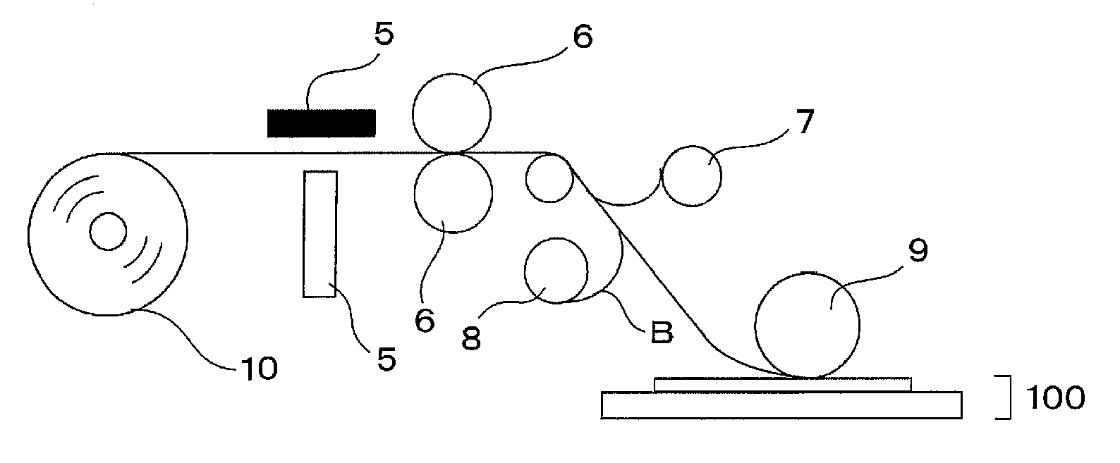
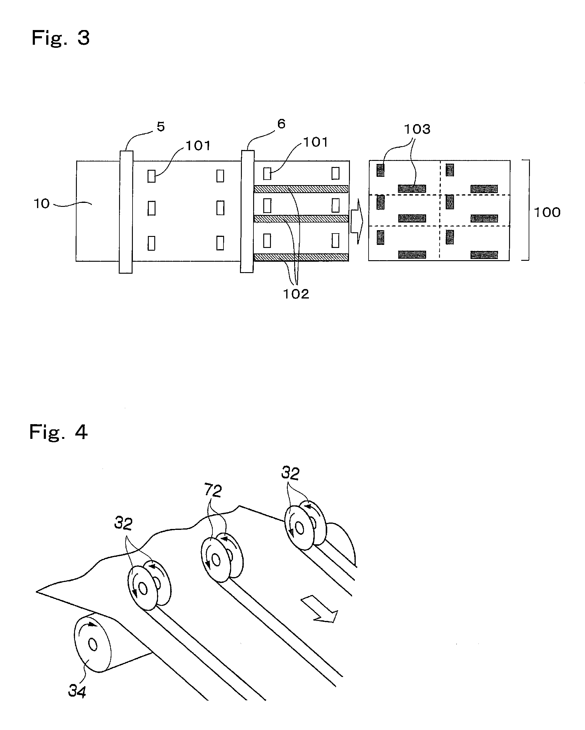
[0088]Using the apparatus shown in FIG. 1, the gas barrier film and the electronic device were bonded through in-line operation. The slitting unit 6 in the apparatus of FIG. 1 has the constitution of FIG. 4.

[0089]Concretely, a roll film composite 1 having a width of 30 cm in the direction perpendicular to the film traveling direction was continuously fed into the blanking unit 5. This was forcedly introduced into the unit and blanked therein in such a manner that the size of each hole 101 could be 1 cm×2 cm (film traveling direction×direction perpendicular to the film traveling direction—the same shall apply hereinunder). In this, the punch in the blanking unit 5 was made to run through the film composite 10 from the side of the gas barrier film 14 thereof and the distance between the punch diameter of the punch and the hole diameter of the die opening (one side clearance) was controlled to be 3μm. Subsequently, this was slit in the slitting unit 6 in such a manner that the slit wid...

example 2

[0095]In the same manner as in Example 1, a gas barrier film 14 was bonded to a substrate of an organic EL array 100; however, in this, the film composite 10 was slit completely from the gas barrier film 14 to the protective film B thereof so that the gas barrier film 14, the adhesive layer 12 and the protective layer B could be all peeled off.

(Evaluation)

[0096]In Examples 1 and 2, the samples were checked for bonding misalignment of the hole 101 and the slit part to be wound off 102 relative to the wire lead-out part 103. In addition, the obtained organic EL devices were evaluated in the manner mentioned below. 10 test pieces were tested in every evaluation test. The evaluation results are shown in Table 1.

[0097]A: Misalignment was within 1 mm.

B: Misalignment was from 1 to 2 mm.

C: Misalignment was from 2 to 5 mm.

D: Misalignment was more than 5 mm, or misalignment stepped over the wire lead-out parts in bonding.

(Evaluation of Light-Emitting Surface Condition of Organic EL Device)

[00...


PUM


Abstract

A method for bonding a gas barrier film and an electronic device, comprising continuously feeding a film composite that contains a gas barrier film having a support and a gas barrier layer, and an adhesive layer; blanking or slitting a part of the film composite to form a wire lead-out part therein; and continuously roll-bonding the film composite to a substrate with an electronic device formed thereon; wherein the feeding of the film composite, the forming of the wire lead-out part and the roll-bonding are carried out through in-line operation.

Description

CROSS-REFERENCE TO RELATED APPLICATIONS[0001]The present application claims the benefit of priority from Japanese Patent Application No. 216706 / 2009, filed on Sep. 18, 2009, the contents of which are herein incorporated by reference in their entirety.BACKGROUND OF THE INVENTION[0002]1. Field of the Invention[0003]The present invention relates to a method for bonding a gas barrier film and an electronic device, to a method for producing an electronic device array that includes the bonding method, and to a method for producing an electronic device that includes the production method. The invention also relates to the electronic device produced according to the electronic device producing method.[0004]2. Description of the Related Art[0005]An electronic device such as an organic EL device requires a wire lead-out part or a lead-out wire (e.g., lead pin) running outward from the electronic device substrate.[0006]Heretofore, in case where a lead-out wire is provided between a pair of sub...

Claims


Application Information

Patent Timeline
IPC IPC(8): H01J1/62B32B38/04
CPCB32B37/223Y10T156/1067B32B2037/268B32B2038/045B32B2307/7242B32B2309/02B32B2309/04B32B2309/105B32B2457/12B32B2457/202B32B2457/208H01L31/048H01L51/0097H01L51/5237H01L51/56Y02E10/549B32B38/04Y02P70/50H10K77/111H10K50/844H10K71/00
Inventor AIBA, SATOSHI
Owner FUJIFILM CORP
Why Eureka
Try Eureka