Ultrasonic probe, method for manufacturing the same and ultrasonic diagnostic apparatus

a technology of ultrasonic probes and ultrasonic diagnostic equipment, which is applied in the direction of mechanical vibration separation, instruments, tomography, etc., can solve the problems of unsolved anti-septic solution turns, cmut chip dysfunction caused by penetration of adhesion agents, and cmut chip dysfunction. , to achieve the effect of preventing cmut chip dysfunction

Inactive Publication Date: 2011-03-24
HITACHI MEDICAL CORP
View PDF3 Cites 42 Cited by
  • Summary
  • Abstract
  • Description
  • Claims
  • Application Information

AI Technical Summary

Benefits of technology

[0041]In this manner, it is possible to provide an ultrasonic diagnostic apparatus capable of preventing dysfunction of a CMUT chip due to penetration of adhesive agent.
[0042]In accordance with the present invention, it is possible to provide an ultrasonic probe, the method for manufacturing the ultrasonic probe and ultrasonic diagnostic apparatus capable of preventing dysfunction of a CMUT chip due to penetration of adhesive agent.

Problems solved by technology

Such configured CMUT probe has a problem that when it is immersed in antiseptic solution such as alcohol, the antiseptic solution turns to solvent of adherent agent.
The penetrated adherent agent hardens a frame body and a film body of the CMUT chip, whereby leading to dysfunction in transmission / reception of ultrasonic waves in the inner space segmented by the hardened frame body and film body.
Such dysfunction of a CMUT chip caused by penetration of adherent agent still remains unsolved.

Method used


Image

  • Ultrasonic probe, method for manufacturing the same and ultrasonic diagnostic apparatus
  • Ultrasonic probe, method for manufacturing the same and ultrasonic diagnostic apparatus
  • Ultrasonic probe, method for manufacturing the same and ultrasonic diagnostic apparatus

Examples


first embodiment

(3. First Embodiment)

[0096]Next, the first embodiment will be described referring to FIG. 5 and FIG. 6.

(3-1. Configuration Member of Ultrasonic Probe 2)

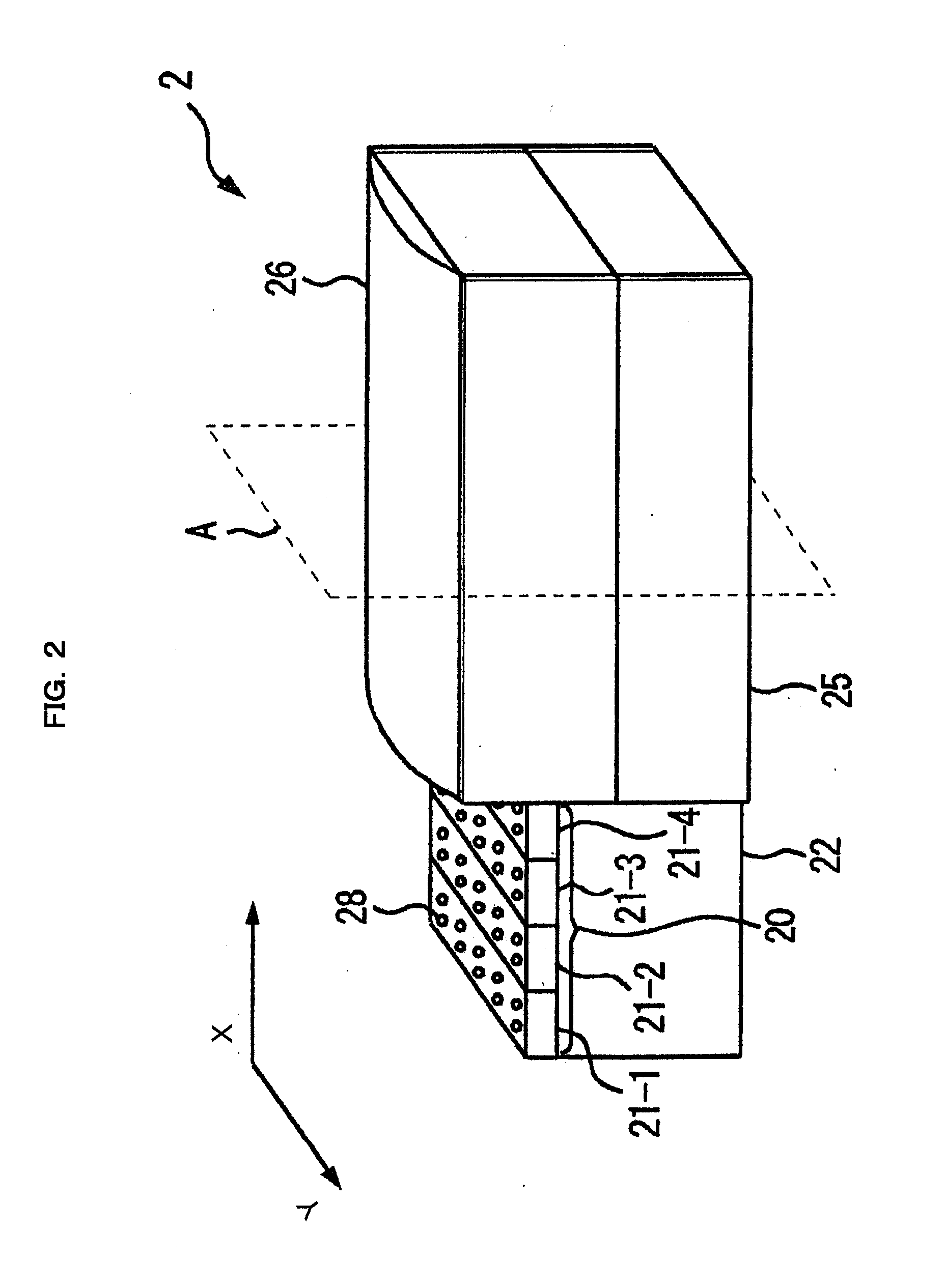
[0097]FIG. 5 shows ultrasonic probe 2 related to the first embodiment. FIG. 5 is a cross-sectional view of plane A of ultrasonic probe 2 shown in FIG. 2.

[0098]Electric conducting layer 76 is formed along the ultrasonic-wave irradiation side of CMUT chip 20 and the side surface of flexible substrate 72 and backing layer 22, and insulating film 78 which is an insulating layer is formed on the inner surface of acoustic lens 26. Electric conducting layer 76 and insulating layer 78 are formed by the method such as vacuum deposition, sputtering or CVD, and electric conducting layer 76 is formed by Cu or AI film having electrical conductivity. Insulating layer 78 is attached to electric conducting layer 76 by adhesive. Insulating layer 78 is formed by silicon oxide film or paraxilene film, etc. and is chemical resistant. Being chemical resi...

second embodiment

(4. Second Embodiment)

[0126]Next, the second embodiment will be described referring to FIG. 7.

[0127]FIG. 7 shows ultrasonic probe 2a related to the second embodiment. FIG. 7 is equivalent to the cross-sectional view of plane A in FIG. 2.

[0128]While electric conducting layer 76 is formed along the ultrasonic-wave irradiation side of CMUT chip 20 and the side surfaces of flexible substrate 72 and backing layer 22 and connected to ground wire 84 via adhesive portion 82 in the first embodiment, insulating film 78a is to be formed as an insulating layer between CMUT chip 20 and electric conducting layer 76 in the second embodiment. In the same manner as embodiment 1, insulating film 78 is formed as an insulating layer on the inner surface of acoustic lens 26.

[0129]In accordance with the second embodiment, dysfunction of CMUT chip due to penetration of adhesive can be prevented as in the first embodiment. Also, since electric conducting layer 76 is provided as the ground layer on the ultr...

third embodiment

(5. Third Embodiment)

[0130]Next, the third embodiment will be described referring to FIG. 8 and FIG. 9.

[0131]FIG. 8 is a pattern diagram showing the wiring of ultrasonic probe 2.

[0132]FIG. 9 shows the ground connection of base plate 40 in CMUT chip 20, and is the cross-sectional view of the B-B line illustrated in FIG. 8.

[0133]In the periphery border of the top surface of CMUT chip 20, upper electrode 46 of CMUT chip 20 and signal pattern 38 of flexible substrate 72 are connected by wire 86-1, and lower electrode 48 of CMUT chip 20 and signal pattern 41 of flexible substrate 72 are connected by wire 86-2. Photo curing resin 88 is filed around wire 86 and the terminal area is sealed.

[0134]In a corner portion of CMUT chip 20, electric conducting resin 89 is filled between CMUT chip 20 and flexible substrate 72. Electric conducting resin 89 is equivalent to the terminal area between base plate 40 of CMUT chip 20 and ground wire 94. Ground wire 94 is disposed between flexible substrate ...


PUM

PropertyMeasurementUnit
thicknessaaaaaaaaaa
thicknessaaaaaaaaaa
voltageaaaaaaaaaa

Abstract

An ultrasonic probe is provided with a CMUT chip having a plurality of transducer elements that change electromechanical coupling coefficients or sensitivities in accordance with a bias voltage to transmit and receive ultrasonic waves, an electric conducting layer formed on the ultrasonic irradiation side of the CMUT chip, an acoustic lens arranged on the ultrasonic irradiation side of the CMUT chip, an insulating layer formed in the direction opposite to the ultrasonic irradiation side of the acoustic lens, a housing unit that stores the CMUT chip in which the electric conducting layer and the insulating layer are fixed with an adhesive and the acoustic lens, wherein the insulating layer is formed by the material that includes at least either silicon oxide or paraxylene to prevent a solvent of the adhesive from soaking into the adhered portion.

Description

FIELD OF THE INVENTION[0001]The present invention relates to an ultrasonic probe, method for manufacturing the ultrasonic probe and ultrasonic diagnostic apparatus.DESCRIPTION OF RELATED ART[0002]An ultrasonic diagnostic apparatus is for imaging a diagnostic image based on the reflected echo signals outputted from an ultrasonic probe. The ultrasonic probe has a plurality of ultrasonic transducers disposed therein. Ultrasonic transducers convert driving signals into ultrasonic waves to transmit them to an object to be examined, and receive the reflected echo signals produced from the object and convert them into electrical signals.[0003]In recent years, ultrasonic probes using a CMUT (Capacitive Micromachined Ultrasonic Transducer) have been developed. The CMUT is an ultrafine capacity-type ultrasonic transducer manufactured by semiconductor microfabrication process. In CMUT, transmission / reception sensitivity of ultrasonic waves, i.e. electromechanical coupling coefficient varies ac...

Claims


Application Information

Patent Timeline
Patent Type & Authority Applications(United States)
IPC IPC(8): A61B8/14G10K9/12H04R31/00
CPCA61B8/06A61B8/13Y10T29/49005B06B1/0292A61B8/4455G01N29/2406
Inventor SANO, SHUZOYOSHIMURA, YASUHIRONAGATA, TATSUYAFUKADA, MAKOTOSAKO, AKIFUMI
Owner HITACHI MEDICAL CORP
Why Eureka
Try Eureka