Three-dimensional semiconductor memory device and method of fabricating the same

a semiconductor memory and three-dimensional technology, applied in the field of can solve the problems of low product reliability, conventional three-dimensional semiconductor memory devices may require unstable processing, and limited pattern miniaturization, and achieve the effect of enhancing process margin and superior reliability

Active Publication Date: 2011-03-31
SAMSUNG ELECTRONICS CO LTD
View PDF7 Cites 259 Cited by
  • Summary
  • Abstract
  • Description
  • Claims
  • Application Information

AI Technical Summary

Benefits of technology

[0008]It is therefore another feature of an embodiment to provide a three-dimensional semiconductor memory device with superior reliability.
[0009]It is y

Problems solved by technology

However, pattern miniaturization may be limited due to extremely expensive semiconductor equipments and/or difficulties in semiconductor fabrication pr

Method used


Image

  • Three-dimensional semiconductor memory device and method of fabricating the same
  • Three-dimensional semiconductor memory device and method of fabricating the same
  • Three-dimensional semiconductor memory device and method of fabricating the same

Examples


embodiment 1

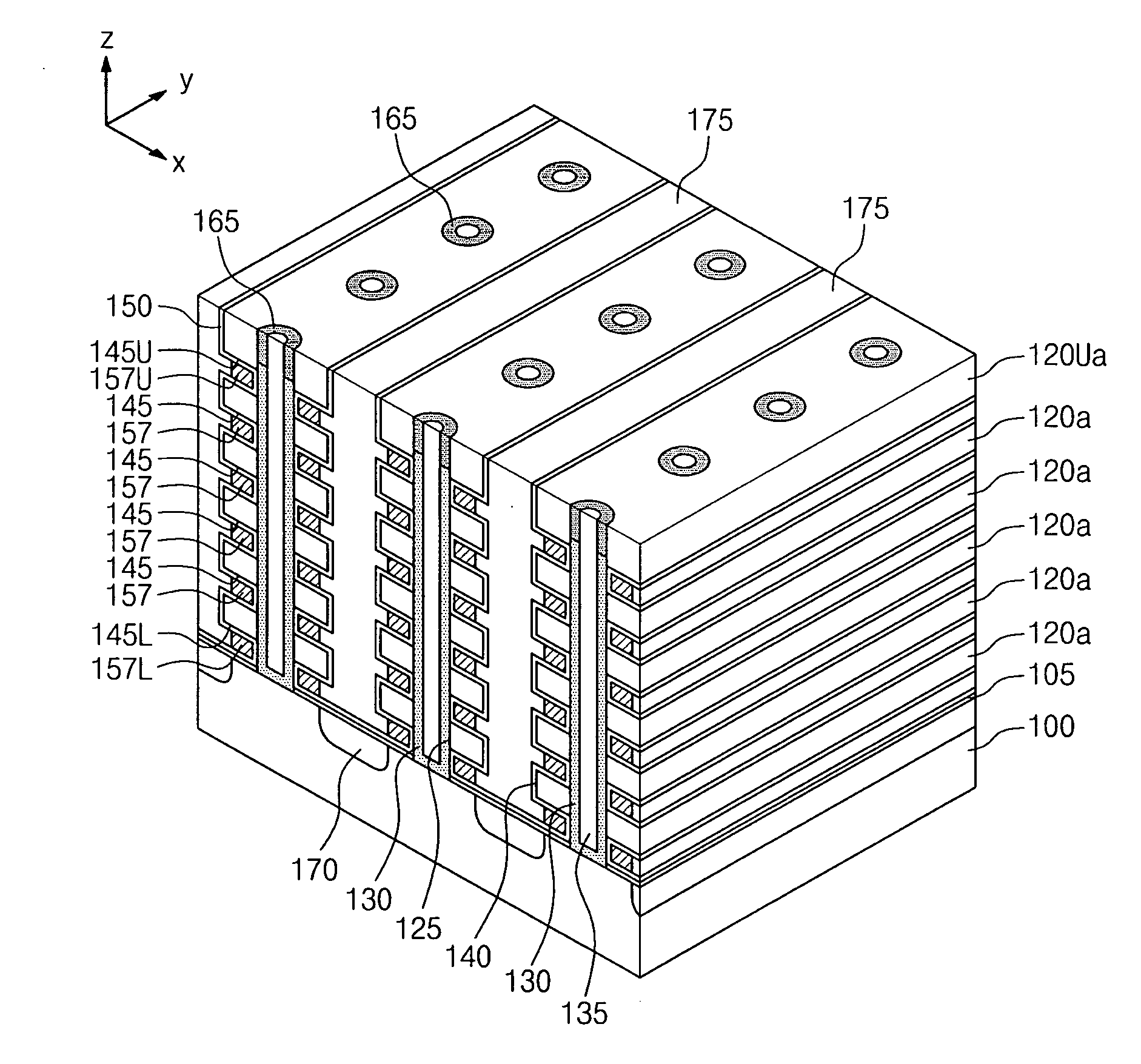
[0035]FIGS. 1 through 8 illustrate perspective views of stages in a method of fabricating a three-dimensional semiconductor memory device according to an embodiment. FIG. 9 illustrates a detailed cross-sectional view of portion A in FIG. 6.

[0036]Referring to FIG. 1, sacrificial layers 110L, 110, 110U and insulating layers 120, 120U may be alternately and repeatedly stacked on a substrate 100. The substrate 100 may be a semiconductor substrate. For example, the substrate 100 may be a silicon substrate, a germanium substrate, a silicon-germanium substrate, a compound semiconductor substrate, or the like. The substrate 100 may be doped with a first conductive type dopant. The sacrificial layers 110L, 110, 110U may be preferably formed of a material having an etch selectivity with respect to the insulating layers 120, 120U. For example, the insulating layers 120, 120U may be formed of oxide, and the sacrificial layers 110L, 100, 110U may include nitride and / or oxy-nitride. The inventive...

embodiment 2

[0076]A three-dimensional semiconductor memory device according to another embodiment may be similar to that described previously with reference to FIGS. 1-13. Accordingly, descriptions of the same elements will not be repeated in detail.

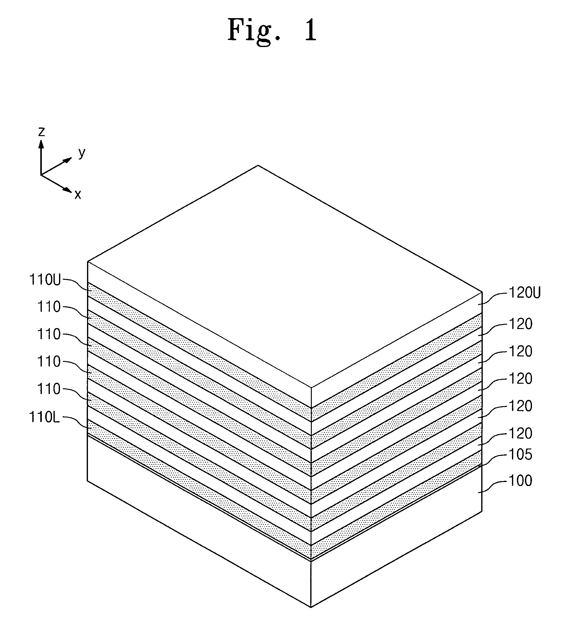
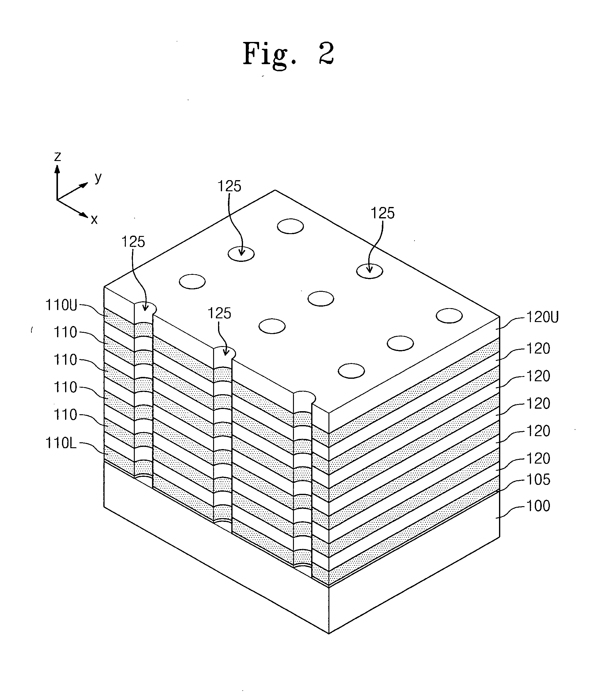
[0077]FIGS. 14 through 17 illustrate perspective views of stages in a method of fabricating a three-dimensional semiconductor memory device according to another embodiment. The method of fabricating the three-dimensional semiconductor memory device according to the present embodiment may include the fabricating stages described with reference to FIGS. 1 through 3.

[0078]Referring to FIGS. 3 and 14, the insulating layers 120U, 120 and the sacrificial layers 110U, 110, 110L may be continuously patterned to form trenches 140a. The trenches 140a may be spaced apart laterally from the channel openings 125. The active patterns 130 may be arranged two-dimensionally in a first direction and a second direction, which may be parallel to a top surface of the su...


PUM


Abstract

A method of fabricating a semiconductor memory device includes alternately and repeatedly stacking sacrificial layers and insulating layers on a substrate, forming an active pattern penetrating the sacrificial layers and the insulating layers, continuously patterning the insulating layers and the sacrificial layers to form a trench, removing the sacrificial layers exposed in the trench to form recess regions exposing a sidewall of the active pattern, forming an information storage layer on the substrate, forming a gate conductive layer on the information storage layer, such that the gate conductive layer fills the recess regions and defines an empty region in the trench, the empty region being surrounded by the gate conductive layer, and performing an isotropic etch process with respect to the gate conductive layer to form gate electrodes in the recess regions, such that the gate electrodes are separated from each other.

Description

BACKGROUND[0001]1. Field[0002]The present disclosure herein relates to a semiconductor device and a method of fabricating the same, and more particularly, to a three-dimensional semiconductor memory device and a method for fabricating the same.[0003]2. Description of the Related Art[0004]As the electronic industry has advanced to a high level, integration density of semiconductor devices has increased. Higher integration density of semiconductor devices is an important factor in determining product price. In other words, as integration density of semiconductor devices increases, product prices of semiconductor devices may decrease. Accordingly, a requirement for higher integration density of semiconductor devices is increasing. Typically, since integration density of semiconductor devices is mainly determined by an area occupied by a unit memory cell, integration may be greatly influenced by a degree of pattern miniaturization, i.e., a level of fine pattern forming technology. Howev...

Claims


Application Information

Patent Timeline
IPC IPC(8): H01L21/8239
CPCH01L27/11551H01L27/11556H01L27/11578H01L27/11582H01L29/42336H01L29/42352H01L21/8239H01L29/66666H01L29/66825H01L29/66833H01L29/7827H01L29/7889H01L29/7926H01L29/4236H10B41/20H10B41/27H10B43/20H10B43/27H01L29/0688
Inventor KIM, JINHOSON, BYOUNGKEUNKIM, HANSOOLEE, WONJUNJANG, DAEHYUN
Owner SAMSUNG ELECTRONICS CO LTD
Why Eureka
Try Eureka