Solid-state image pickup device, method for manufacturing the same, and electronic apparatus

a pickup device and solid-state technology, applied in the direction of electrical equipment, semiconductor devices, radio frequency controlled devices, etc., can solve the problems of reducing light use efficiency and sensitivity, and achieve the effects of low cost, high-quality images, and efficient manufacturing

Active Publication Date: 2011-04-07
SONY CORP
View PDF1 Cites 12 Cited by
  • Summary
  • Abstract
  • Description
  • Claims
  • Application Information

AI Technical Summary

Benefits of technology

[0029]The present invention can provide a solid-state image pickup device and an electronic apparatus that can be efficiently manufactured at low

Problems solved by technology

In the surface emission type, unfortunately, conductor lines are disposed in a plurality of layers in the path through which light enters the photo

Method used


Image

  • Solid-state image pickup device, method for manufacturing the same, and electronic apparatus
  • Solid-state image pickup device, method for manufacturing the same, and electronic apparatus
  • Solid-state image pickup device, method for manufacturing the same, and electronic apparatus

Examples


first embodiment

1. First Embodiment

(A) Structure

(A-1) Structure of Principal Part of Camera

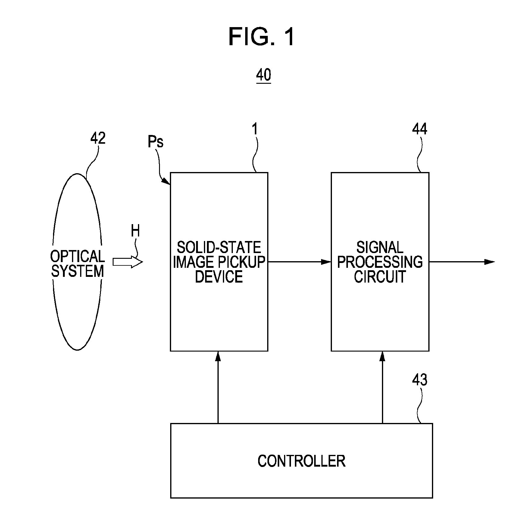
[0055]FIG. 1 is a block diagram of a camera 40 according to a first embodiment of the present invention.

[0056]As shown in FIG. 1, the camera 40 includes a solid-state image pickup device 1, an optical system, 42, a controller 43, and a signal processing circuit 44. These elements will be described one by one.

[0057]The solid-state image pickup device 1 receives light (subject image) H coming through the optical system 42 at an image pickup face Ps and converts the light into electricity to generate a signal charge. In the present embodiment, the solid-state image pickup device 1 is operated according to control signals output from the controller 43. More specifically, the solid-state image pickup device 1 reads out the signal charge and output it as raw data.

[0058]The optical system 42 includes optical members, such as an image-forming lens and an iris, which are arranged so that the light H of the subject ima...

second embodiment

2. Second Embodiment

(A) Structure

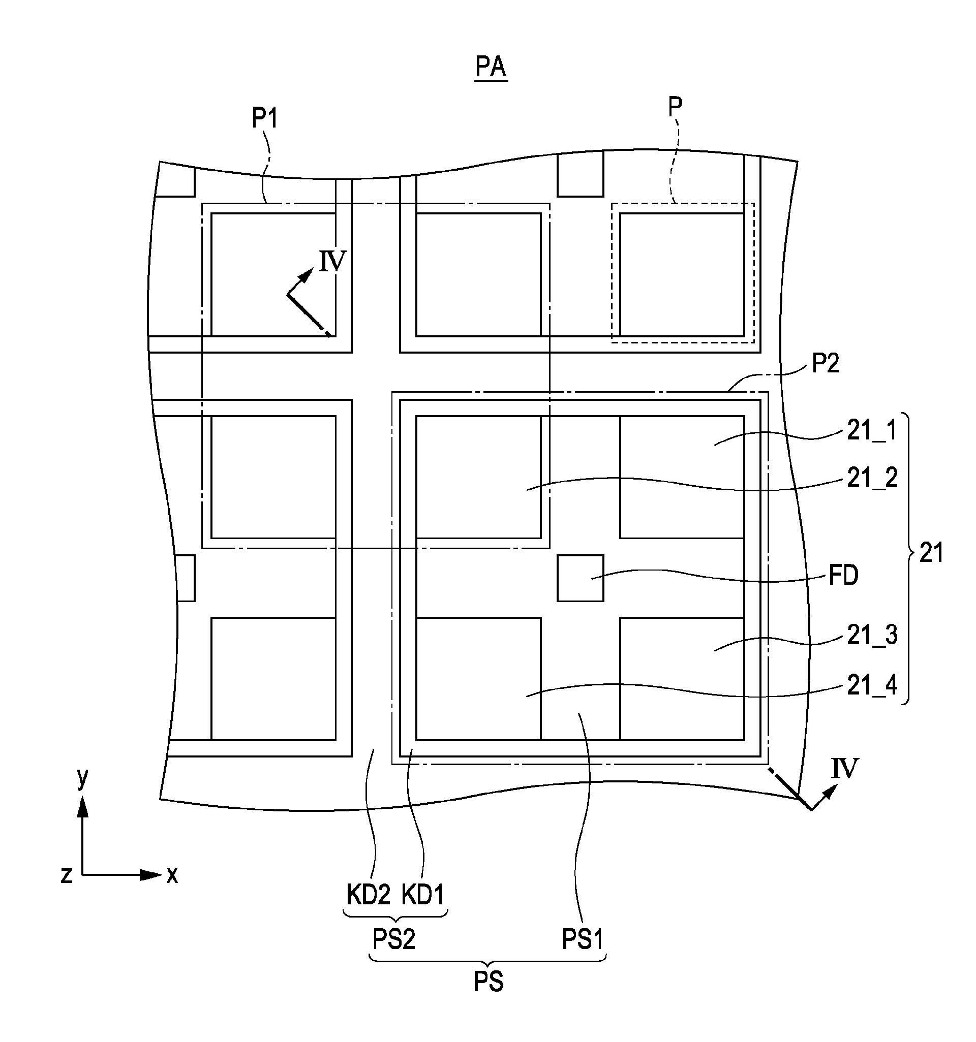
[0198]FIGS. 14 and 15 are fragmentary views of a principal part of a solid-state image pickup device according to a second embodiment of the present invention.

[0199]FIG. 14 is a schematic top view similar to FIG. 3 showing a principal part of an image pickup region PA. FIG. 15 is a schematic sectional view similar to FIG. 4 showing a principal part of the image pickup region PA. FIG. 14 shows the substrate 101 shown in FIG. 15. FIG. 15 shows the section taken along line XV-XV in FIG. 14.

[0200]In the present embodiment, the pixel isolation member PSb is different from that of the first embodiment, as shown in FIGS. 14 and 15. The present embodiment is the same as the first embodiment except for the pixel isolation member, and the same descriptions will be omitted.

[0201]As shown in FIGS. 14 and 15, the pixel isolation member PSb includes a first pixel isolation member PS1 and a second pixel isolation member PS2, as in the first embodiment. Unlike the f...


PUM


Abstract

A method for manufacturing a solid-state image pickup device is provided. In this method, a pixel isolation member is formed in a semiconductor substrate including pixels, and the thickness of the substrate is reduced by CMP. For forming the pixel isolation member, a first pixel isolation member is formed by implanting impurity ions in a region of the substrate so that the pixels are disposed between portions of the region when viewed from a surface of the substrate. A second isolation member is also formed by forming a trench in a region of the substrate different from the first pixel isolation member so that the pixels are disposed between portions of the region, and then filling the trench with an electroconductive material harder to polish by CMP than the substrate. The CMP is performed on the rear side of the substrate using the second pixel isolation member as a stopper.

Description

BACKGROUND OF THE INVENTION[0001]1. Field of the Invention[0002]The present invention relates to a solid-state image pickup device, a method for manufacturing the same, and an electronic apparatus.[0003]2. Description of the Related Art[0004]Electronic apparatuses, such as digital video cameras and camera-equipped cellular phones, include solid-state image pickup devices.[0005]The solid-state image pickup device has an image-pick up region including a plurality of pixels on a semiconductor substrate. Each pixel has a photoelectric conversion portion. The photoelectric conversion portion, which may be a photodiode, generates a signal charge by receiving light coming through an external optical system and converting the light to electricity.[0006]A CMOS (complementary metal oxide semiconductor) image sensor can be used as the solid-state image pickup device.[0007]The CMOS image sensor includes pixels, each including the photoelectric conversion portion and a set of transistors. The se...

Claims


Application Information

Patent Timeline
IPC IPC(8): H01L27/14H01L31/18
CPCH01L27/14621H01L27/14641H01L27/1463
Inventor NISHIZAWA, KENICHITAKAHASHI, HIROSHI
Owner SONY CORP
Why Eureka
Try Eureka