Liquid crystal display device and electronic device including the same
- Summary
- Abstract
- Description
- Claims
- Application Information
AI Technical Summary
Benefits of technology
Problems solved by technology
Method used
Image

Examples
embodiment 1
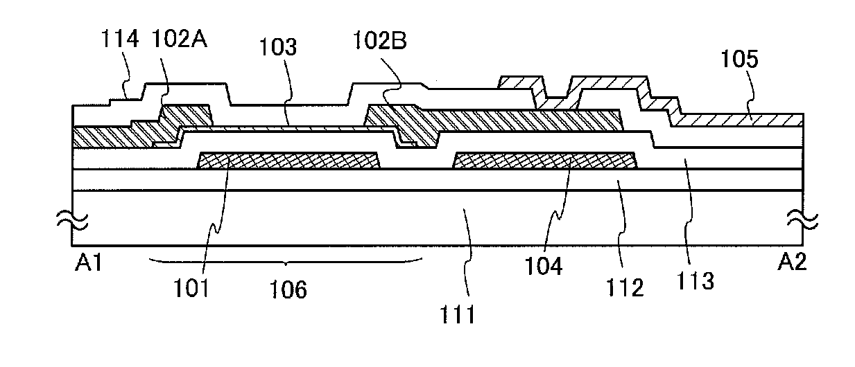
[0029]In this embodiment, a liquid crystal display device will be described using a thin film transistor (hereinafter also referred to as a TFT) and an electrode functioning as a pixel electrode (such an electrode is also simply referred to as a pixel electrode) connected to the TFT, as an example. Note that a pixel refers to an element group that is composed of elements provided in each pixel of a display device, for example, an element for controlling display in accordance with an electric signal, such as a thin film transistor, an electrode functioning as a pixel electrode, or a wiring. A pixel may include a color filter or the like and may correspond to one color component whose brightness can be controlled with one pixel. Therefore, for example, in a color display device including color elements of R, G, and B, a minimum unit of an image is composed of three pixels of an R pixel, a G pixel, and a B pixel and an image can be obtained with a plurality of pixels.
[0030]Note that wh...
embodiment 2
[0091]An example in which a pixel in a display device includes a TFT having a structure different from that in Embodiment 1 will be described below.
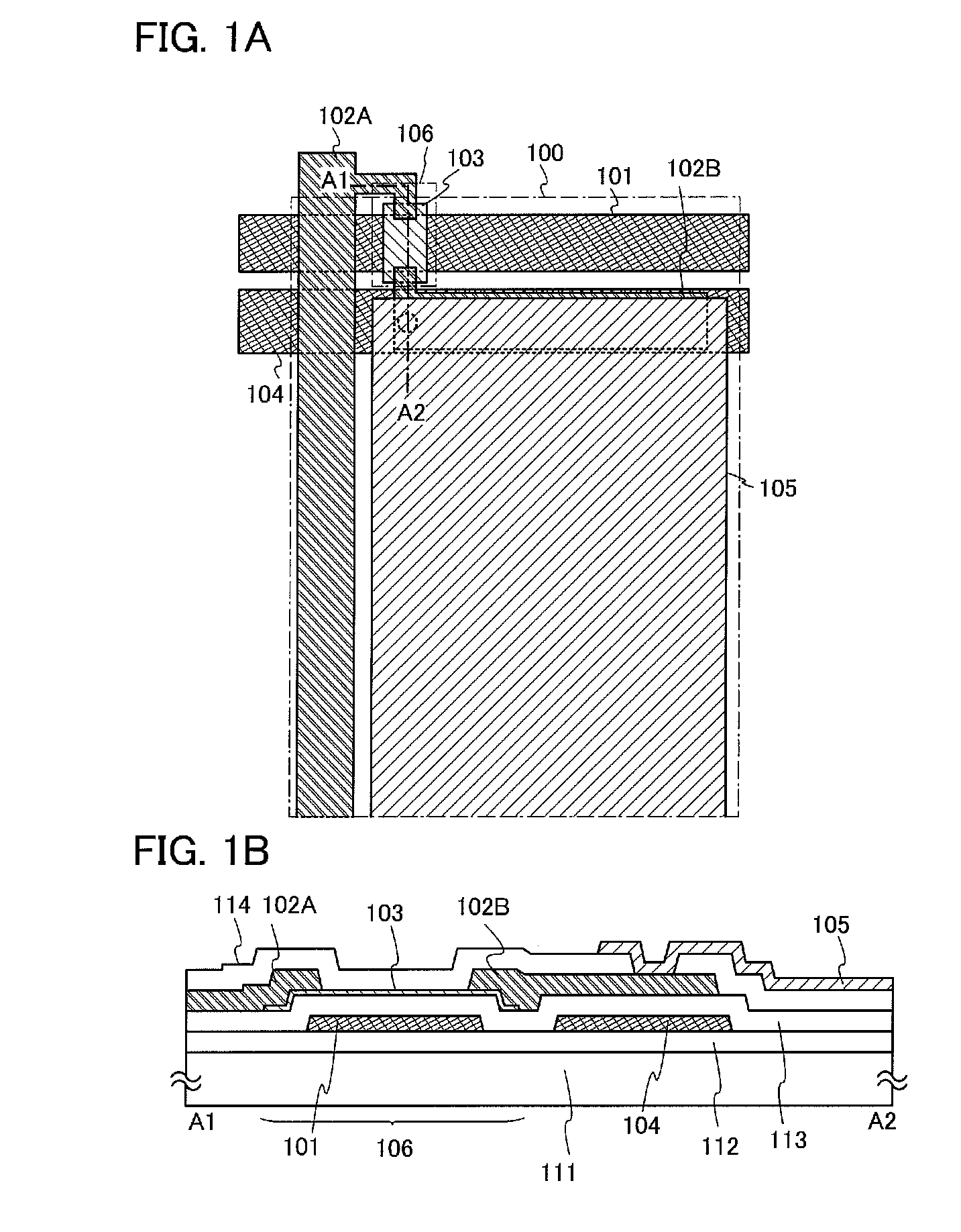
[0092]FIG. 4A is a top view of a pixel having a structure different from that in Embodiment 1. A TFT illustrated in FIG. 4A is a kind of bottom-gate structure called an inverted staggered structure in which a wiring layer serving as a source electrode and a drain electrode of the TFT is placed opposite to an oxide semiconductor layer serving as a channel region, with respect to a wiring serving as a gate.
[0093]A pixel 400 illustrated in FIG. 4A includes a first wiring 401 functioning as a scan line, a second wiring 402A functioning as a signal line, an oxide semiconductor layer 403, a capacitor line 404, and a pixel electrode 405. Moreover, the pixel 400 includes a third wiring 402B for electrically connecting the oxide semiconductor layer 403 and the pixel electrode 405, so that a thin film transistor 406 is formed. The first wiring 401...
embodiment 3
[0105]An example in which a pixel in a display device includes a TFT having a structure different from those in Embodiments 1 and 2 will be described below.
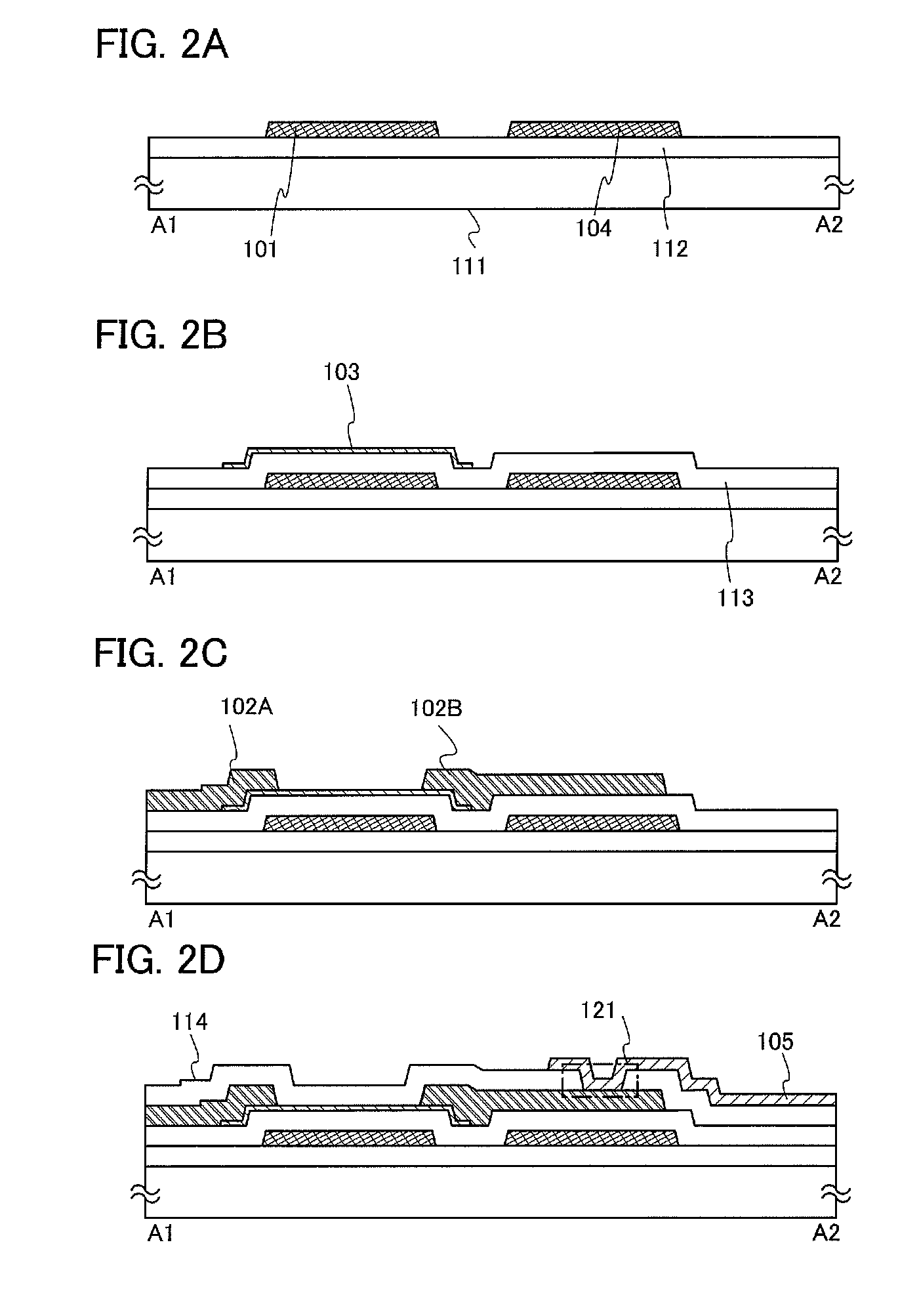
[0106]FIGS. 6A to 6C are a top view and cross-sectional views of a pixel that has a structure different from that in Embodiment 2. Note that the structure in the top view of FIG. 6A is similar to that of FIG. 4A; therefore, the description is not repeated. The structure in the cross-sectional view of FIG. 6B is different from the structure in the cross-sectional view of FIG. 4B in that an insulating layer 601A is provided between the first wiring 401 and the second wiring 402A, and that an insulating layer 601B is provided between the first wiring 401 and the third wiring 402B. FIG. 6C is a cross-sectional view along dashed line B1-B2 in FIG. 6A and illustrates a structure in which the insulating layer 601A is placed between the capacitor line 404 and the second wiring 402A.
[0107]When the second wiring 402A and the third wiring 4...
PUM
 Abstract
Description
Claims
Application Information
 - R&D Engineer
- R&D Manager
- IP Professional
- Industry Leading Data Capabilities
- Powerful AI technology
- Patent DNA Extraction
Browse by: Latest US Patents, China's latest patents, Technical Efficacy Thesaurus, Application Domain, Technology Topic.
© 2024 PatSnap. All rights reserved.Legal|Privacy policy|Modern Slavery Act Transparency Statement|Sitemap