Exposure apparatus, exposure method, and device manufacturing method

a technology of exposure apparatus and manufacturing method, which is applied in the direction of photomechanical treatment, printing, instruments, etc., can solve the problems of weaker intensity of 450 mm wafer compared to 300 mm wafer, and difficulty in putting wafer carriage into practice in the same way and means as in the current 300 mm wafer, so as to achieve the effect of increasing size and weigh

Inactive Publication Date: 2011-04-14
NIKON CORP
View PDF8 Cites 18 Cited by
  • Summary
  • Abstract
  • Description
  • Claims
  • Application Information

AI Technical Summary

Benefits of technology

[0009]According to this apparatus, the carrier system loads the object on the movable body as well as unloads the object from the movable body, using the chuck member which holds the object from above in a non-contact manner. Accordingly, members and the like to load / unload the object on / from the movable body do not have to be provided, which can keep the movable body from increasing in size and weight. Further, by using the chuck member which holds the wafer from above in a non-contact manner, a thin, flexible object can be loaded onto the movable body as well as unloaded from the movable body without any problems.
[0012]According to this apparatus, the carrier system loads the object on the movable body as well as unloads the object from the movable body, using the chuck member which holds the object from above in a non-contact manner. Accordingly, members and the like to load / unload the object on / from the movable body do not have to be provided, which can keep the movable body from increasing in size and weight. Further, by using the chuck member which holds the wafer from above in a non-contact manner, a thin, flexible object can be loaded onto the movable body as well as unloaded from the movable body without any problems.

Problems solved by technology

However, because the thickness of the wafer does not increase in proportion to the size of the wafer, intensity of the 450 mm wafer is much weaker when compared to the 300 mm wafer.
Accordingly, even when addressing an issue such as wafer carriage, it is anticipated that putting wafer carriage into practice in the same ways and means as in the current 300 mm wafer Would be difficult.

Method used


Image

  • Exposure apparatus, exposure method, and device manufacturing method
  • Exposure apparatus, exposure method, and device manufacturing method
  • Exposure apparatus, exposure method, and device manufacturing method

Examples


Embodiment Construction

[0035]An embodiment of the present invention will be described below, with reference to FIGS. 1 to 19.

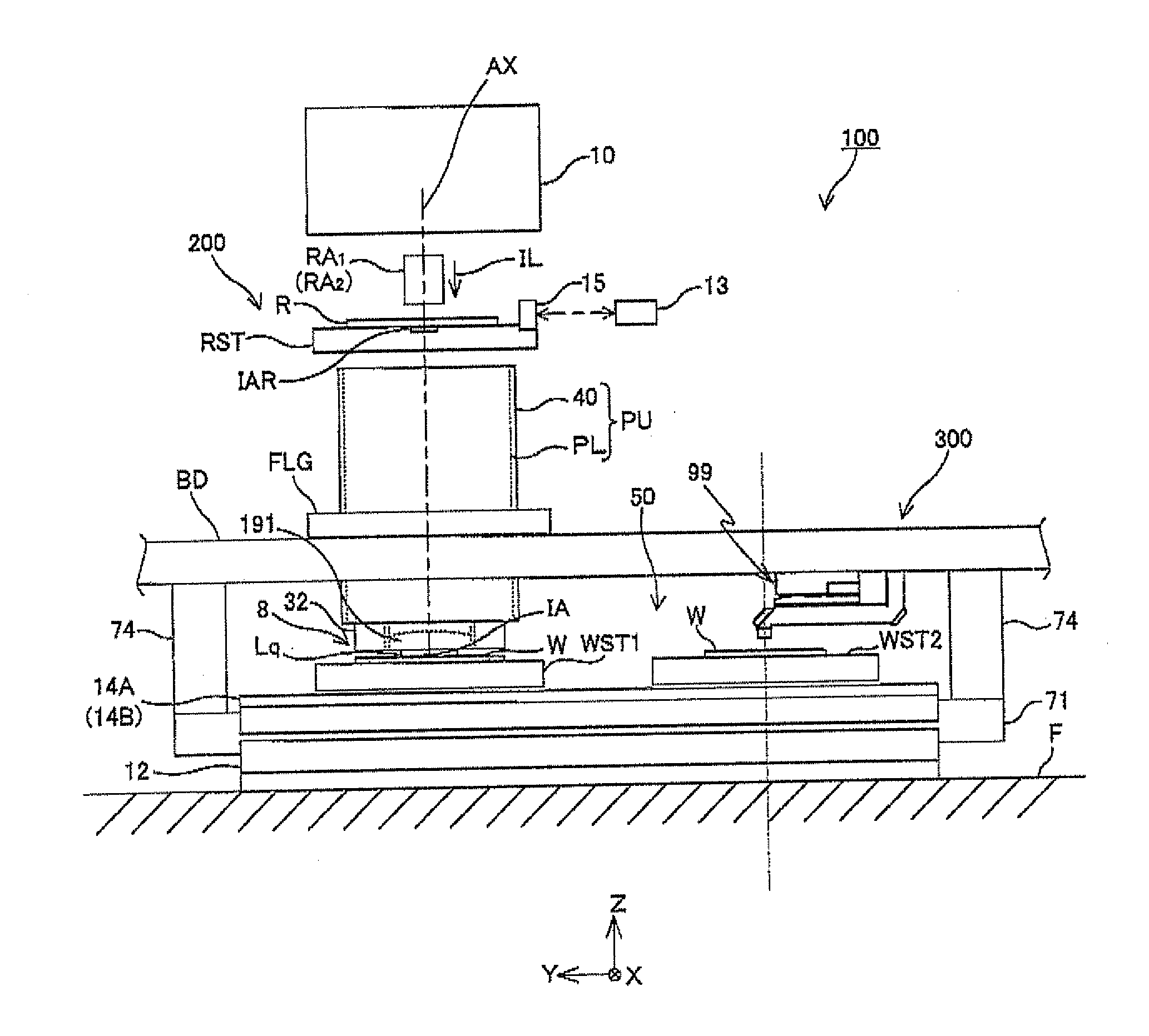
[0036]FIG. 1 schematically shows a configuration of an exposure apparatus 100 related to the embodiment. Exposure apparatus 100 is a projection exposure apparatus by a step-and-scan method, which is a so-called scanner. As described later on, a projection optical system PL is provided in the present embodiment, and in the description below, the explanation is given assuming that a direction parallel to an optical axis AX of projection optical system PL is a Z-axis direction, a direction in which a reticle and a wafer are relatively scanned within a plane orthogonal to the Z-axis direction is a Y-axis direction, and a direction orthogonal to the Z-axis and the I-axis is an X-axis direction, and rotational (tilt) directions around the X-axis, Y-axis and Z-axis are θx, θy and θz directions, respectively.

[0037]As shown in FIG. 1, exposure apparatus 100 is equipped with an exposure stati...


PUM


Abstract

A wafer is loaded on a wafer stage and unloaded from a wafer stage, using a chuck member which holds the wafer from above in a non-contact manner. Accordingly, members and the like to load / unload the wafer on / from the wafer stage do not have to be provided, which can keep the stage from increasing in size and weight. Further, by using the chuck member which holds the wafer from above in a non-contact manner, a thin, flexible wafer can be loaded onto the wafer stage as well as unloaded from the wafer stage without any problems.

Description

CROSS-REFERENCE TO RELATED APPLICATIONS[0001]This non-provisional application claims the benefit of Provisional Application No. 61 / 247,105 filed Sep. 30, 2009, the disclosure of which is hereby incorporated herein by reference in its entirety.BACKGROUND OF THE INVENTION[0002]1. Field of the Invention[0003]The present invention relates to exposure apparatuses and device manufacturing methods, and more particularly to an exposure apparatus in which an object is exposed with an energy beam via an optical system, and a device manufacturing method which uses the exposure apparatus.[0004]2. Description of the Background Art[0005]Conventionally, in a lithography process for manufacturing electron devices (microdevices) such as semiconductor devices (integrated circuits or the like) or liquid crystal display elements, an exposure apparatus such as a projection exposure apparatus by a step-and-repeat method (a so-called stepper), or a projection exposure apparatus by a step-and-scan method (...

Claims


Application Information

Patent Timeline
Patent Type & Authority Applications(United States)
IPC IPC(8): G03B27/54
CPCG03F7/7075G03F7/707G03F7/20H01L21/683
Inventor ICHINOSE, GO
Owner NIKON CORP
Why Eureka
Try Eureka