Quantum Infrared Sensor and Quantum Infrared Gas Concentration Meter Using the Same
- Summary
- Abstract
- Description
- Claims
- Application Information
AI Technical Summary
Benefits of technology
Problems solved by technology
Method used
Image
Examples
example 1
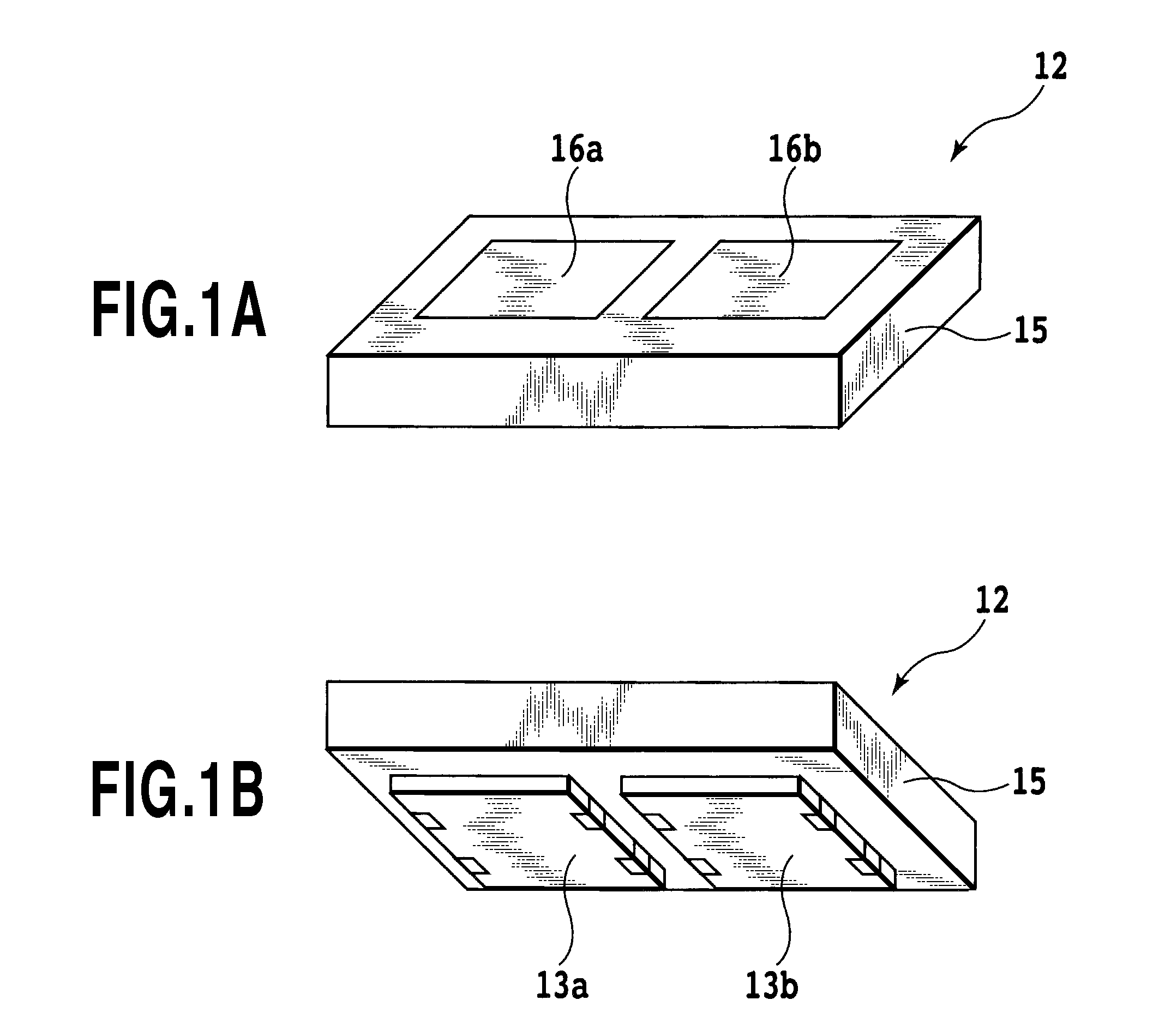
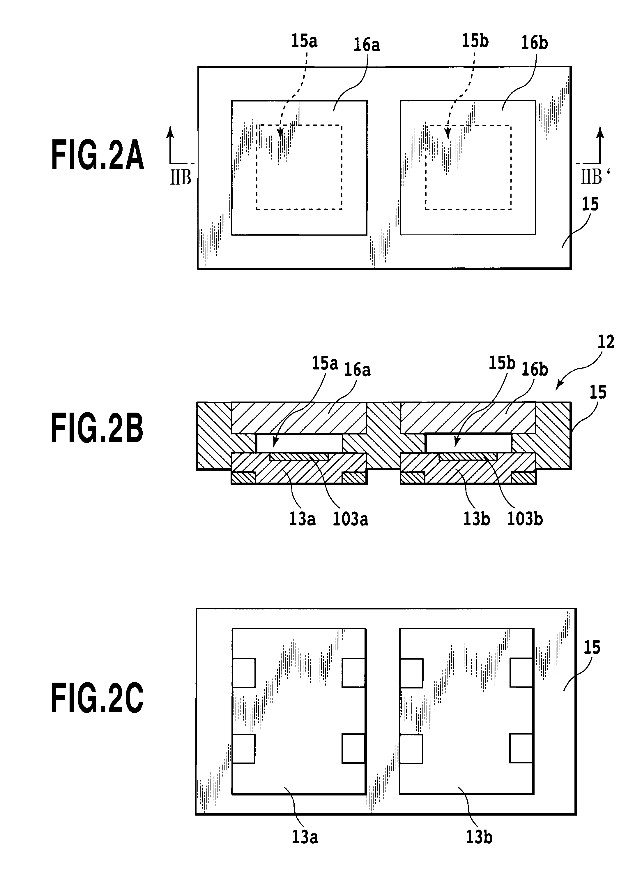
[0059]FIGS. 1A and 1B and FIGS. 2A to 2C are configuration diagrams of a quantum infrared sensor according to the present invention in the case of Example 1. FIG. 1A is a top perspective view, and FIG. 1B is a bottom perspective view. FIGS. 2A to 2C show top, cross-sectional and bottom views, respectively. Note that, FIG. 2B is a cross-sectional view taken along the line IIB-IIB′ in FIG. 2A.
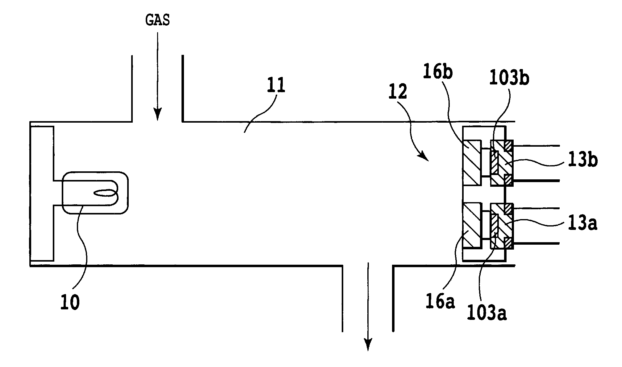
[0060]A quantum infrared sensor 12 according to the present invention includes multiple quantum infrared sensor elements 13a and 13b, multiple optical filters 16a and 16b and a holding frame 15. The multiple optical filters 16a and 16b, are provided for the infrared sensor elements 13a and 13b, respectively, on the side directed to the infrared light source. The multiple optical filters 16a and 16b are configured to selectively transmit infrared rays in specific different wavelength ranges, respectively. The holding frame 15, which includes multiple through holes 15a and 15b, holds at least these...
example 2
[0089]FIGS. 4A and 4B and FIGS. 5A to 5C are configuration diagrams of a quantum infrared sensor according to the present invention in the case of Example 2. FIG. 4A is a top perspective view, and FIG. 4B is a bottom perspective view. FIGS. 5A to 5C show top, cross-sectional and bottom views, respectively. Note that, FIG. 5B is a cross-sectional view taken along the line VB-VB′ in FIG. 5A. In the drawings, reference signs 13a to 13d denote quantum infrared sensor elements, respectively, and reference signs 16a to 16d denote optical filters, respectively.
[0090]Example 2 illustrates an example in which four quantum infrared sensor elements and four optical filters are employed, the elements and filters employed in Example 1 shown in FIGS. 1A and 1B and FIGS. 2A to 2C.
[0091]The four optical filters 16a to 16d are formed of one optical filter that transmits reference light from the infrared light source, and three optical filters that transmit light rays in wavelength ranges each differ...
example 3
[0094]FIG. 6 is a configuration diagram without the gaps between the optical filters and the quantum infrared sensor elements shown in FIG. 2B and FIG. 5B. That is, it is possible to employ a structure in which the optical filters 16a and 16b and the quantum infrared sensor elements 13a and 13b are arranged in close contact with each other while the gaps therebetween are eliminated. In addition, the optical filters 16a and 16b can be attached to the holding frame 15 after the quantum infrared sensor elements 13a and 13b are attached to the holding frame 15. With the quantum infrared sensor according to the present invention, no gaps need to be provided between the optical filters 16a and 16b and the quantum infrared sensor elements 13a and 13b as in the case of Example 3. Accordingly, an infrared sensor further reduced in size and thickness can be achieved.
PUM
 Abstract
Description
Claims
Application Information
 - R&D
- Intellectual Property
- Life Sciences
- Materials
- Tech Scout
- Unparalleled Data Quality
- Higher Quality Content
- 60% Fewer Hallucinations
Browse by: Latest US Patents, China's latest patents, Technical Efficacy Thesaurus, Application Domain, Technology Topic, Popular Technical Reports.
© 2025 PatSnap. All rights reserved.Legal|Privacy policy|Modern Slavery Act Transparency Statement|Sitemap|About US| Contact US: help@patsnap.com


