Method for Stacked Contact with Low Aspect Ratio

a technology of stacked contact and aspect ratio, applied in the field of integrated circuits, can solve the problems of unexpected circuit degradation, and lack of proper scaling, etc., and achieve the effect of reducing the aspect ratio of the contact plug and reducing the shortening of the top corner of the contact plug

Active Publication Date: 2011-04-21
TAIWAN SEMICON MFG CO LTD
View PDF17 Cites 11 Cited by
  • Summary
  • Abstract
  • Description
  • Claims
  • Application Information

AI Technical Summary

Benefits of technology

[0012]The advantageous features of the present invention include reducing aspect ratio of contact plugs, and reducing top corner shortening of the contact plugs. The bottom profile of the contact plugs may also be improved.

Problems solved by technology

This lack of proper scaling incurs several problems.
Therefore, top corners of contact plugs 6 may be shortened, partially due to optical proximity effects and the inaccurate control of the etching processes.
High aspect ratio also results in difficulties in the control of the bottom profile of contact openings, which in turn results in unexpected circuit degradation, and even device failure.

Method used


Image

  • Method for Stacked Contact with Low Aspect Ratio
  • Method for Stacked Contact with Low Aspect Ratio
  • Method for Stacked Contact with Low Aspect Ratio

Examples


first embodiment

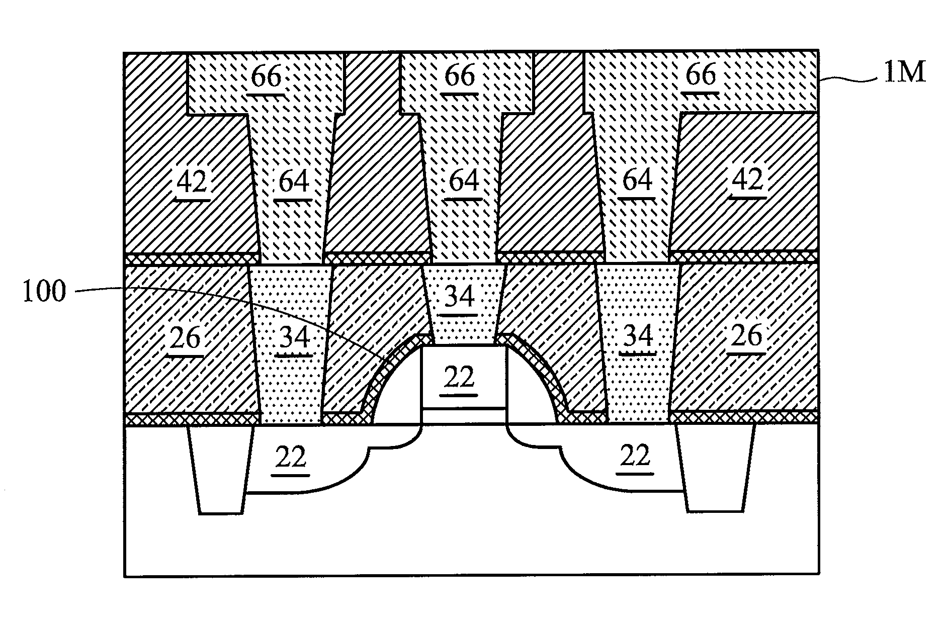
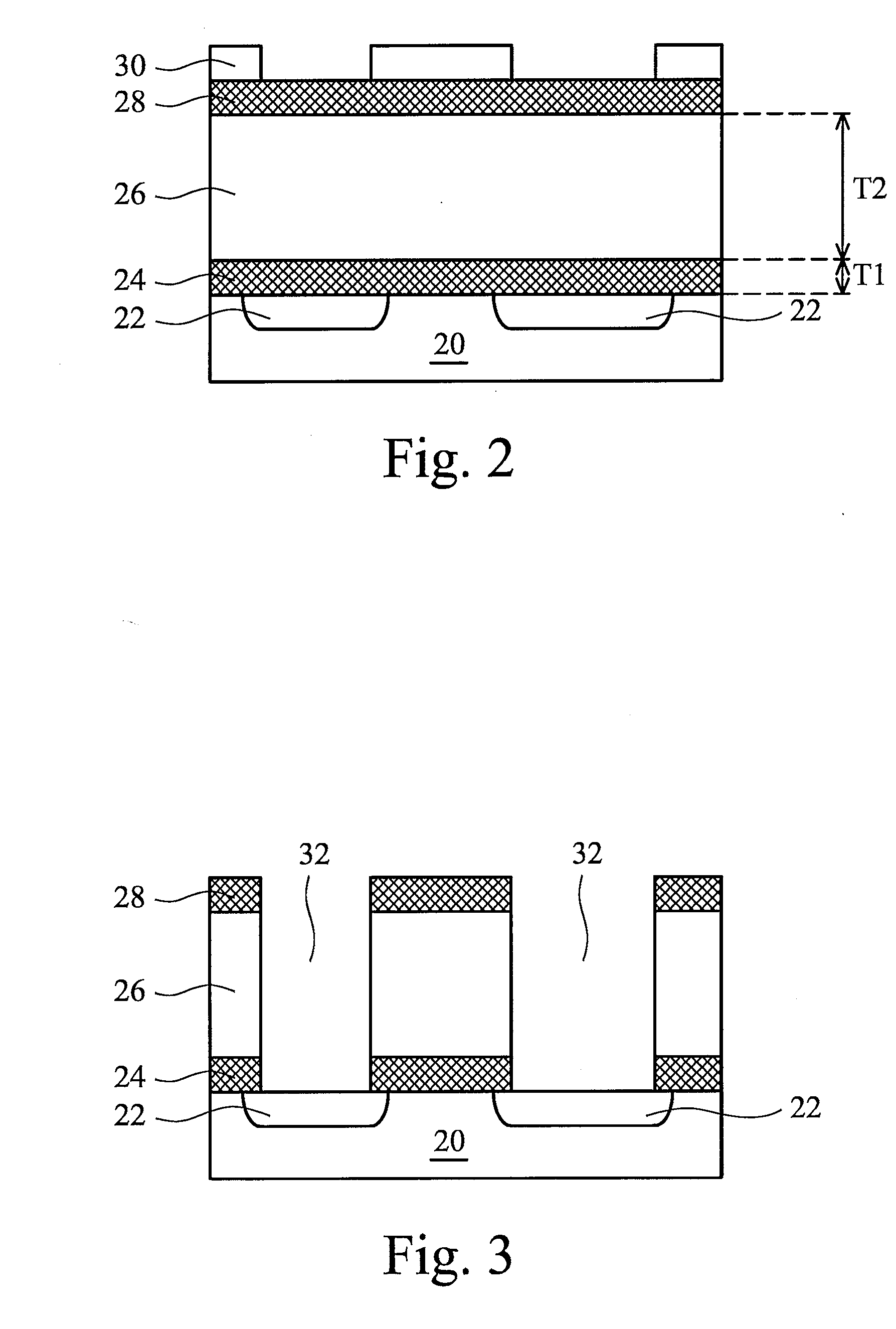
[0020]FIGS. 2 through 9 illustrate cross-sectional views of the present invention. Referring to FIG. 2, substrate 20 is provided. Substrate 20 is preferably a semiconductor substrate, which may include single crystalline semiconductor materials such as silicon, or compound materials having commonly used group III, group IV and group V elements. Regions 22 are illustrated to symbolize semiconductor device components, which will be in contact with the subsequently formed contact plugs. Regions 22 may be source and drain regions (or the corresponding silicide regions) of transistors, contact pads of resistors, and silicide regions. Also, regions 22 symbolize contact regions formed over substrate 20, such as gate electrodes, plates of capacitors, and corresponding silicide regions.

[0021]Etch stop layer (ESL) 24 is formed over substrate 20 and regions 22. In an embodiment, ESL 24 includes silicon nitride. In other embodiments, ESL 24 includes other commonly used dielectric materials, suc...

second embodiment

[0031]FIGS. 10 through 13 illustrate the present invention, wherein single damascene processes are used to form upper contact plugs and the bottom metallization layer M1. The initial process steps are essentially the same as shown in FIGS. 2 through 4. Next, as shown in FIG. 10, ESL 70, ILD 72, DARC 74 and photoresist 76 are sequentially formed, wherein the thickness of ESL 70 and ILD 72 are preferably the same as thicknesses T3 and T4 as in FIG. 5, respectively. ILD 72 may include essentially the same materials as dielectric portion 421 (refer to FIG. 9). Photoresist 76 is then patterned.

[0032]Next, as shown in FIG. 11, contact openings 78 are formed, exposing lower contact plugs 34. Width W2 of contact openings 78 may be greater than, equal to, or smaller than width W1 of lower contact plugs 34, and both are preferably less than about 50 nm. Referring to FIG. 12, contact openings 78 are filled with conductive materials to form upper contact plugs, which include contact liners 82 a...


PUM


Abstract

A method for an integrated circuit structure includes providing a semiconductor substrate; forming a metallization layer over the semiconductor substrate; forming a first dielectric layer between the semiconductor substrate and the metallization layer; forming a second dielectric layer between the semiconductor substrate and the metallization layer, wherein the second dielectric layer is over the first dielectric layer; and forming a contact plug with an upper portion substantially in the second dielectric layer and a lower portion substantially in the first dielectric layer. The contact plug is electrically connected to a metal line in the metallization layer. The contact plug is discontinuous at an interface between the upper portion and the lower portion.

Description

[0001]This application is a continuation of U.S. patent application Ser. No. 11,706,553, filed Feb. 13, 2007, and entitled “Stacked Contact with Low Aspect Ratio”, which application is hereby incorporated herein by reference in its entirety.TECHNICAL FIELD[0002]This invention relates generally to integrated circuits, and more particularly to the formation of contact plugs connecting semiconductor devices and metallization layers.BACKGROUND[0003]In modern integrated circuits, semiconductor devices are formed on semiconductor substrates, and are connected through metallization layers. The metallization layers are interconnected to the semiconductor devices through contact plugs. Also, external pads are connected to the semiconductor devices through the contact plugs.[0004]FIG. 1 illustrates conventional plugs for connecting the semiconductor devices to the metallization layers. Transistor 4, which symbolizes the semiconductor devices, is formed on semiconductor substrate 2. Inter-laye...

Claims


Application Information

Patent Timeline
Patent Type & Authority Applications(United States)
IPC IPC(8): H01L21/60
CPCH01L21/76808H01L23/485H01L2924/0002H01L23/5226H01L2924/00
Inventor YU, CHEN-HUAYEH, CHEN-NANYAO, CHIH-HSIANGWAN, WEN-KAICHENG, JYE-YEN
Owner TAIWAN SEMICON MFG CO LTD
Why Eureka
Try Eureka