Strained Semiconductor Using Elastic Edge Relaxation, a Buried Stressor Layer and a Sacrificial Stressor Layer

a technology of elastic edge relaxation and semiconductor, applied in the direction of semiconductor devices, basic electric elements, electrical appliances, etc., can solve the problem of channel mobility reduction

Active Publication Date: 2011-04-21
ACORN TECH INC
View PDF22 Cites 50 Cited by
  • Summary
  • Abstract
  • Description
  • Claims
  • Application Information

AI Technical Summary

Problems solved by technology

Threading dislocations represent extended defects and give rise to multiple undesirable consequences in MOSFETs including source / drain junction leakage, reduction of channel mobility, variability of threshold voltage and enhanced diffusion paths leading to potential drain-to-source shorting in short-channel MOSFETs.

Method used


Image

  • Strained Semiconductor Using Elastic Edge Relaxation, a Buried Stressor Layer and a Sacrificial Stressor Layer
  • Strained Semiconductor Using Elastic Edge Relaxation, a Buried Stressor Layer and a Sacrificial Stressor Layer
  • Strained Semiconductor Using Elastic Edge Relaxation, a Buried Stressor Layer and a Sacrificial Stressor Layer

Examples


Embodiment Construction

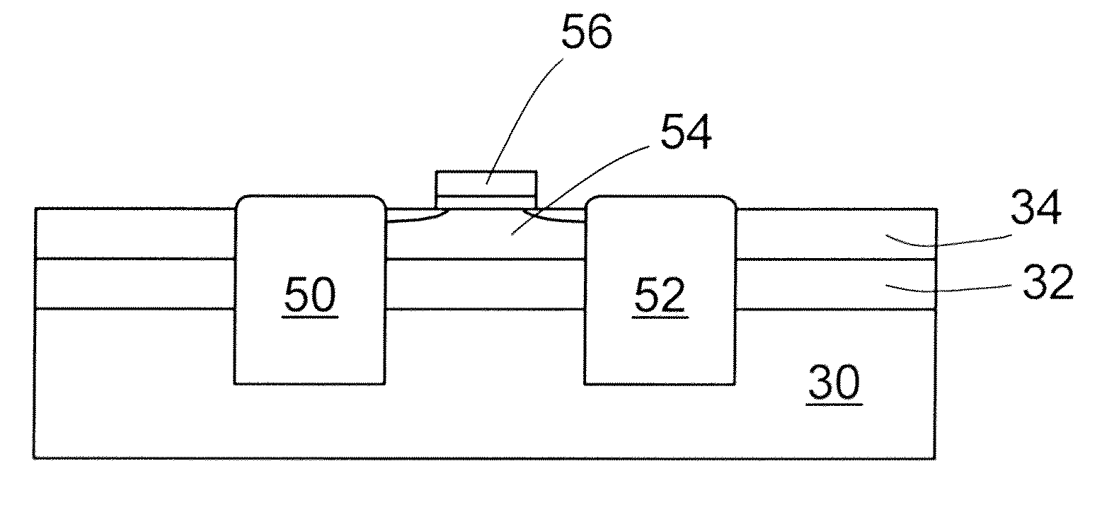
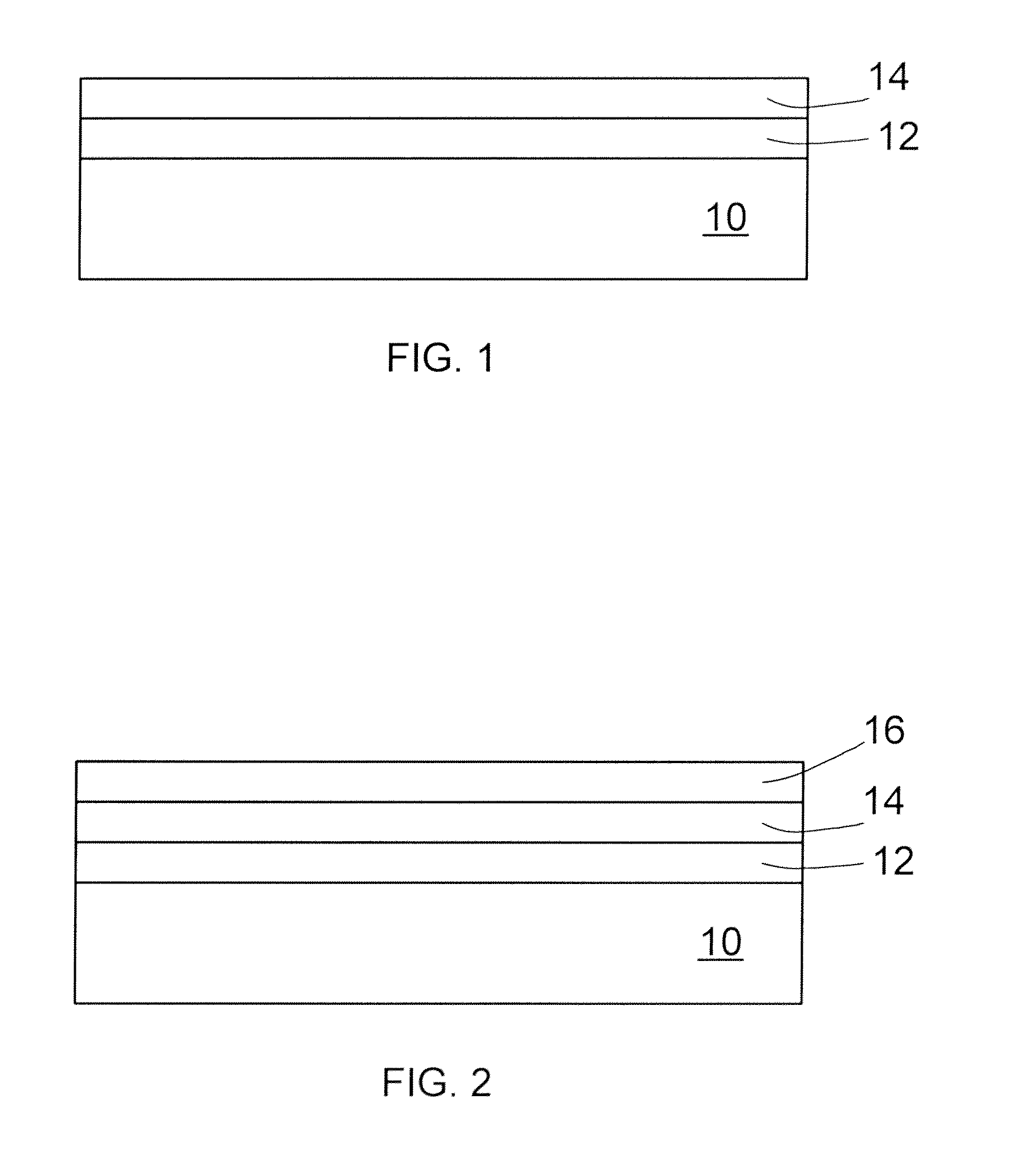
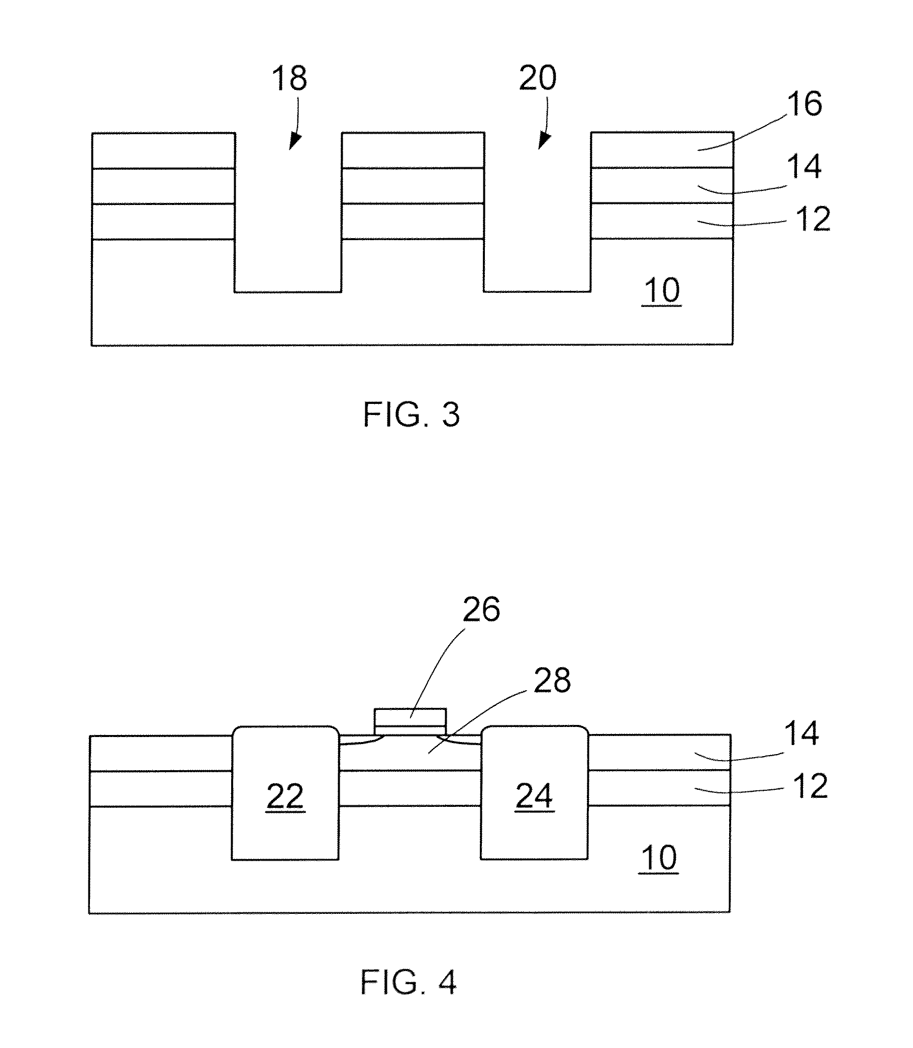
[0009]An aspect of the present invention provides a method of manufacturing a semiconductor device, comprising providing a substrate, forming a buried stressor layer over the substrate and forming an active layer over the buried stressor layer. The buried stressor layer is between the substrate and the active layer. The buried stressor layer is formed in a stressed state in comparison to its equilibrium state. The method continues by forming a sacrificial stressor layer over the active layer, the sacrificial stressor layer formed in a stressed state in comparison to its equilibrium state. Trenches are etched through the active layer, through the buried stressor layer and into at least a portion of the substrate to provide a strained active region defined laterally on at least two sides by trench walls.

[0010]Another aspect of the invention provides a method of manufacturing a semiconductor device, comprising providing a substrate, forming a buried stressor layer over the substrate an...


PUM


Abstract

The present invention relates to creating an active layer of strained semiconductor using a combination of buried and sacrificial stressors. That is, a process can strain an active semiconductor layer by transferring strain from a stressor layer buried below the active semiconductor layer and by transferring strain from a sacrificial stressor layer formed above the active semiconductor layer. As an example, the substrate may be silicon, the buried stressor layer may be silicon germanium, the active semiconductor layer may be silicon and the sacrificial stressor layer may be silicon germanium. Elastic edge relaxation is preferably used to efficiently transfer strain to the active layer.

Description

CROSS REFERENCE TO RELATED APPLICATIONS[0001]This is a divisional application of U.S. patent application Ser. No. 12 / 209,957, filed on Sep. 12, 2008, entitled Strained Semiconductor Using Elastic Edge Relaxation, a Buried Stressor Layer and a Sacrificial Stressor Layer, which application is incorporated by reference in its entirety.BACKGROUND[0002]1. Field of the Invention[0003]The present invention relates to strained semiconductor devices that incorporate strained active layers. The invention also relates to methods of making strained semiconductor devices using a sacrificial stressor layer.[0004]2. Description of the Related Art[0005]Strained silicon is widely viewed as an important technology for obtaining desired advancements in integrated circuit performance. Mobility enhancement results from a combination of reduced effective carrier mass and reduced intervalley (phonon) scattering. For MOS field effect transistors (MOSFETs) fabricated on conventional {100} oriented Si substr...

Claims


Application Information

Patent Timeline
Patent Type & Authority Applications(United States)
IPC IPC(8): H01L21/762
CPCH01L21/0245H01L21/02532H01L21/02664H01L29/7846H01L29/1054H01L29/78H01L21/76224
Inventor GAINES, R. STOCKTONCONNELLY, DANIEL J.CLIFTON, PAUL A.
Owner ACORN TECH INC
Why Eureka
Try Eureka