STI stressor integration for minimal phosphoric exposure and divot-free topography

a stressor and phosphoric exposure technology, applied in the field of shallow trench isolation stressor structures in mosfet devices, can solve the problems of unacceptably high defect rate of current process used to fabricate these devices, and high junction capacitance and junction leakag

Inactive Publication Date: 2007-10-25
FREESCALE SEMICON INC
View PDF8 Cites 41 Cited by
  • Summary
  • Abstract
  • Description
  • Claims
  • Application Information

AI Technical Summary

Problems solved by technology

Since SiGe has a lower energy gap and higher dielectric constant, this leads to higher junction capacitances and junction leakage.
Despite the aforementioned advantages of strained SOI MOSFETs, the fabrication of these devices is beset by certain challenges.
In particular, the processes currently used to fabricate these devices generate an unacceptably high number of defects, especially in the NMOS and PMOS regions of these devices.

Method used


Image

  • STI stressor integration for minimal phosphoric exposure and divot-free topography
  • STI stressor integration for minimal phosphoric exposure and divot-free topography
  • STI stressor integration for minimal phosphoric exposure and divot-free topography

Examples


Embodiment Construction

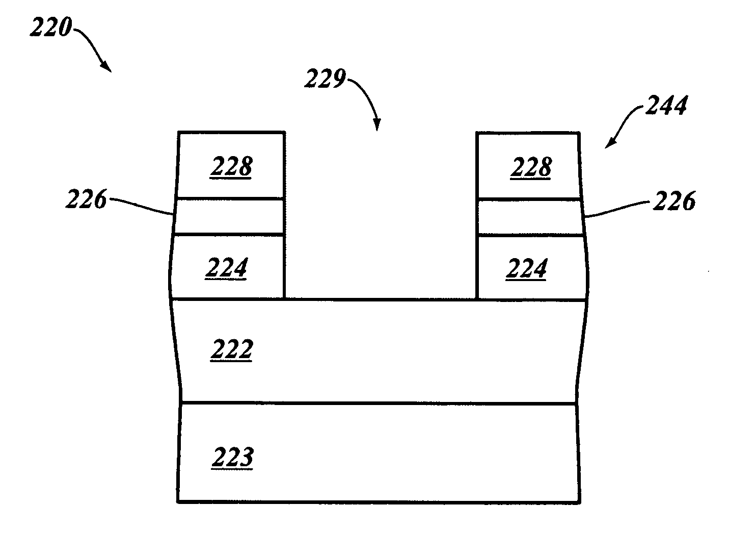
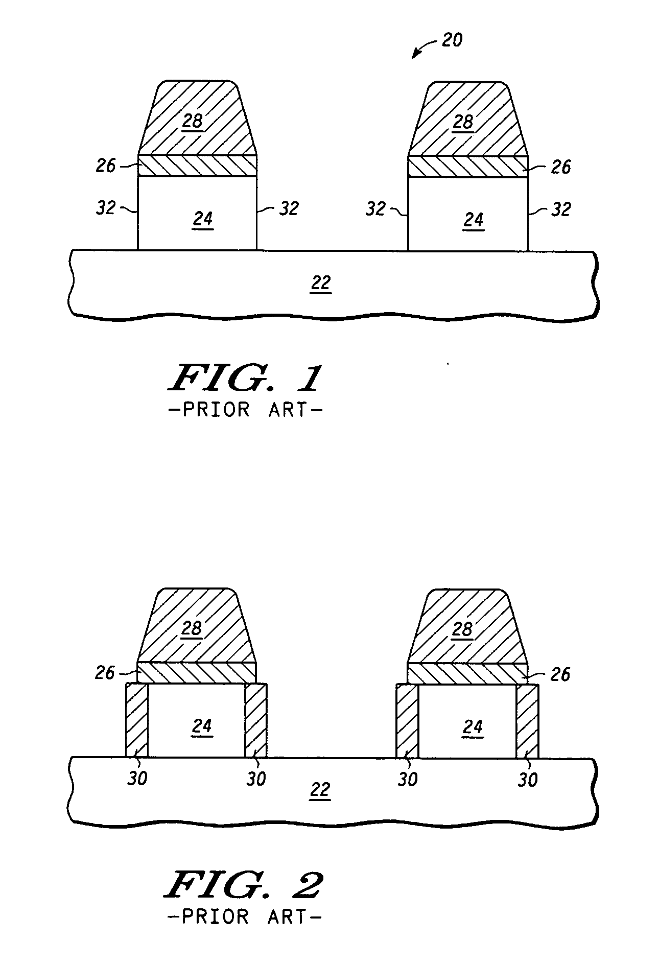
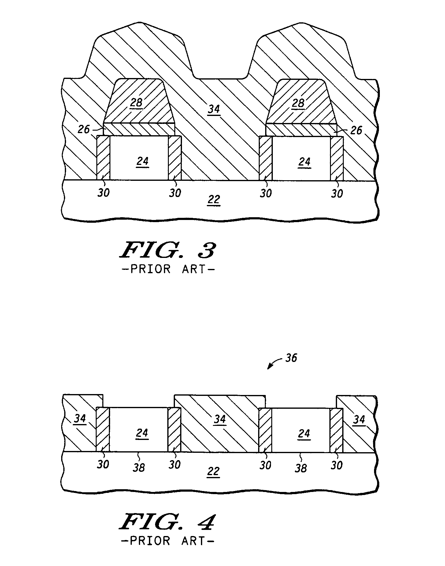
[0025] In one aspect, a method for making a semiconductor device is provided. In accordance with the method, a substrate is provided which comprises an active semiconductor layer disposed on a buried dielectric layer. A trench is created in the substrate which exposes a portion of the buried dielectric layer, and a nitride layer is formed over the surfaces of the trench. The trench is backfilled with an oxide, and the oxide is subjected to densification at a maximum densification temperature of less than about 1200° C.

[0026] In another aspect, a method for making a semiconductor device is provided. In accordance with the method, a semiconductor structure is provided which comprises (a) an active semiconductor layer disposed on a buried dielectric layer, (a) a pad oxide layer disposed over the active semiconductor layer, and (c) a nitride mask disposed over the pad oxide layer. A trench is created in the substrate which extends through the nitride mask, the pad oxide layer and the a...


PUM


Abstract

A method for making a semiconductor device is provided herein. In accordance with the method, a semiconductor structure is provided which comprises an active semiconductor layer (224) disposed on a buried dielectric layer (222). A trench (229) is created in the semiconductor structure which exposes a portion of the buried dielectric layer. An oxide layer (250) is formed over the surfaces of the trench, and at least one stressor structure (254) is formed over the oxide layer.

Description

FIELD OF THE DISCLOSURE [0001] The present disclosure relates generally to semiconductor devices, and more particularly to methods for forming shallow trench isolation (STI) stressor structures in MOSFET devices to enhance their performance. BACKGROUND OF THE DISCLOSURE [0002] The use of silicon-on-insulator (SOI) wafers in making MOSFET devices has become common in the art. In an SOI wafer, a semiconductor layer is provided which is disposed over a buried oxide (BOX) layer. SOI MOSFET transistors offer improvements over bulk MOSFET transistors in terms of circuit speed, reductions in chip power consumption, and in channel-length scaling. These advantages arise at least in part from the decreased junction capacitance made possible by the presence in these devices of a dielectric layer under the active semiconductor region. [0003] The use of a thin layer of strained silicon in the channel layer of MOSFET devices has also been found to improve the performance characteristics of these ...

Claims


Application Information

Patent Timeline
Patent Type & Authority Applications(United States)
IPC IPC(8): H01L21/762
CPCH01L21/76224
Inventor HALL, MARK D.BECKAGE, PETER J.HACKENBERG, JOHN J.VAN GOMPEL, TONI D.
Owner FREESCALE SEMICON INC
Why Eureka
Try Eureka