Method for fabricating a semiconductor device with self-aligned stressor and extension regions

a stressor region and self-aligning technology, applied in the direction of semiconductor devices, basic electric elements, electrical equipment, etc., can solve the problems of affecting the yield, performance and minimum operating voltage characteristics of chips and/or wafers, and affecting the alignment of offset spacers with the boundary of stressor regions

Inactive Publication Date: 2010-02-25
GLOBALFOUNDRIES INC
View PDF8 Cites 39 Cited by
  • Summary
  • Abstract
  • Description
  • Claims
  • Application Information

AI Technical Summary

Benefits of technology

[0010]This summary is provided to introduce a selection of concepts in a simplified form that are further described below in the detailed description. This summary is not intended to identify key features or essential features of the claimed subject matter, nor is it intended to be used as an aid in determining the scope of the claimed subject matter.

Problems solved by technology

Variations in the offset spacer boundary relative to the boundary of the stressor regions can have negative effects on device characteristics.
Non-uniformity across the chip and / or wafer can potentially affect the yield, performance, and minimum operating voltage characteristics of the chip and / or wafer.
As the stressor regions are formed closer to the channel, it becomes difficult to align the offset spacer with the boundary of the stressor regions.
Because the DDS and the offset spacer are formed using separate deposition and etch processes, it is difficult to align the offset spacer with the boundary of the stressor regions.
Additionally, in CMOS devices, the offset spacer is often used as an ion implantation mask during creation of extension implants for both the PMOS and NMOS transistor devices, which limits the ability to resize the offset spacer thickness for purposes of aligning the source / drain extensions for only one of the transistors.
However, these approaches add complexity and cost and still provide an imperfect solution.

Method used


Image

  • Method for fabricating a semiconductor device with self-aligned stressor and extension regions
  • Method for fabricating a semiconductor device with self-aligned stressor and extension regions
  • Method for fabricating a semiconductor device with self-aligned stressor and extension regions

Examples


Embodiment Construction

[0013]The following detailed description is merely illustrative in nature and is not intended to limit the embodiments of the subject matter or the application and uses of such embodiments. As used herein, the word “exemplary” means “serving as an example, instance, or illustration.” Any implementation described herein as exemplary is not necessarily to be construed as preferred or advantageous over other implementations. Furthermore, there is no intention to be bound by any expressed or implied theory presented in the preceding technical field, background, brief summary or the following detailed description.

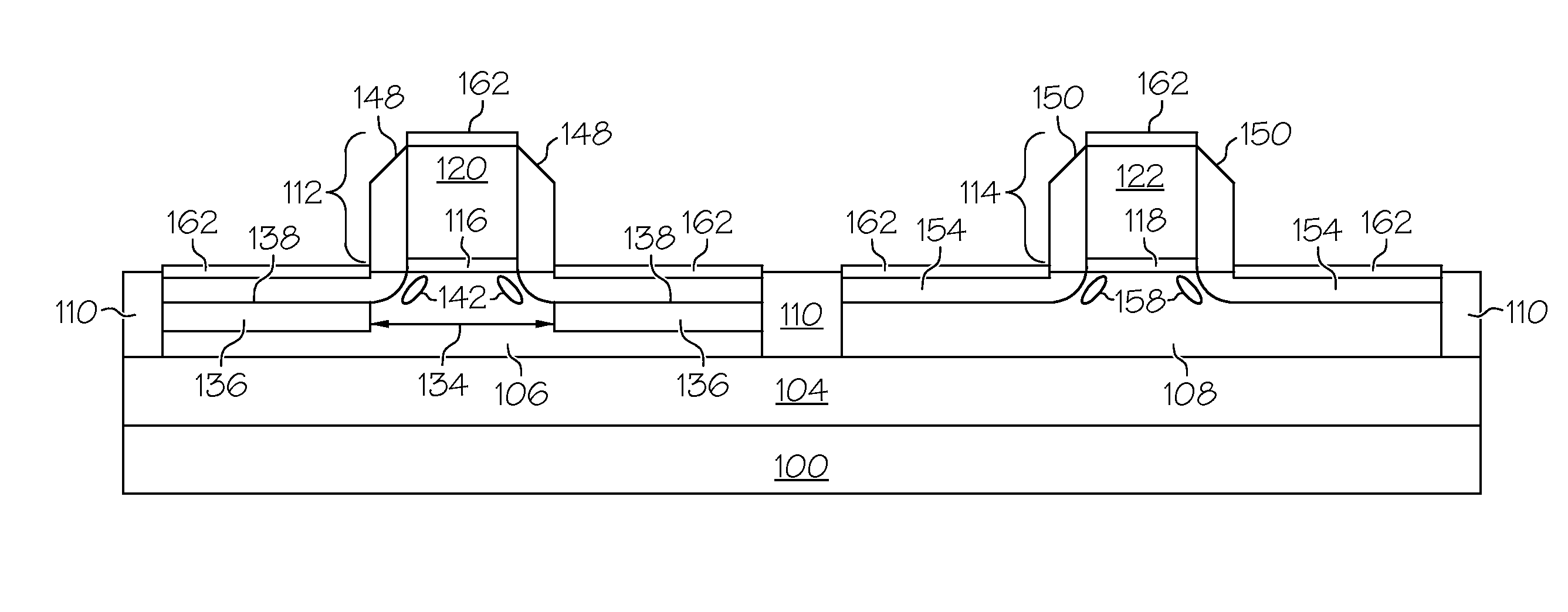
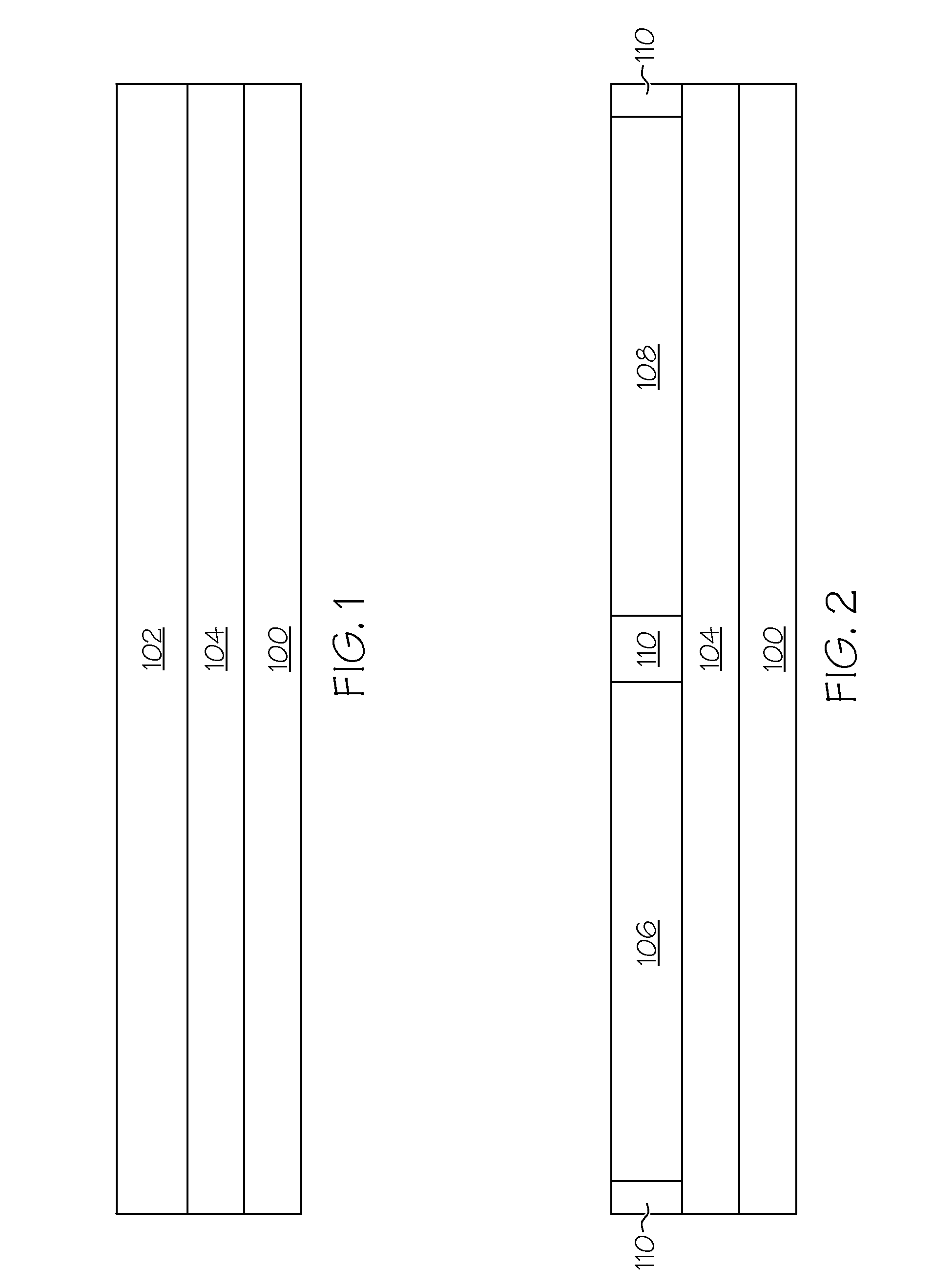
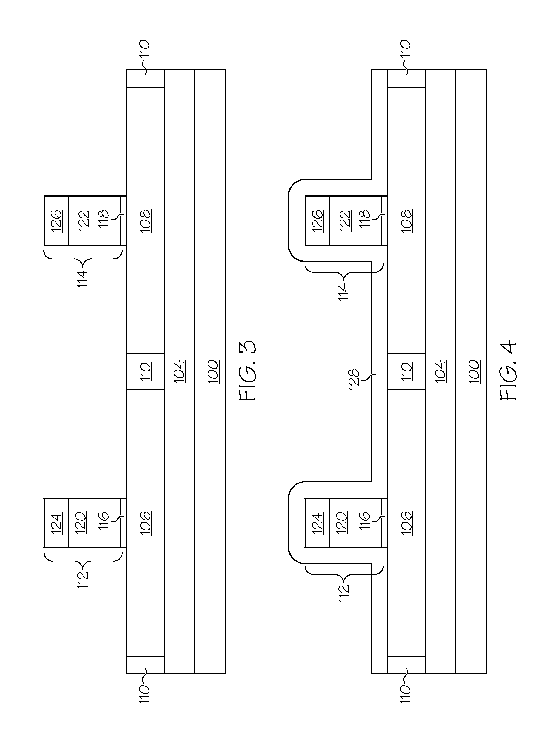
[0014]FIGS. 1-12 illustrate, in cross section, methods for fabricating a CMOS semiconductor device in accordance with exemplary embodiments. Various steps in the manufacture of MOS components are well known and so, in the interest of brevity, many conventional steps will only be mentioned briefly herein or will be omitted entirely without providing the well known process details...


PUM

PropertyMeasurementUnit
thicknessaaaaaaaaaa
thicknessaaaaaaaaaa
thicknessaaaaaaaaaa

Abstract

Methods are provided for fabricating a MOS transistor having self-aligned stressor and extension regions. A method comprises forming a gate stack overlying a layer of semiconductor material and forming a spacer about sidewalls of the gate stack. The method further comprises forming cavities in the layer of semiconductor material, wherein the cavities are substantially aligned with the spacer. The method further comprises forming a stress-inducing semiconductor material in the cavities, and implanting ions of a conductivity-determining impurity type into the stress-inducing semiconductor material using the gate stack and the spacer as an implantation mask.

Description

TECHNICAL FIELD[0001]The present disclosure generally relates to semiconductor devices and methods for fabricating semiconductor devices, and more particularly, embodiments of the subject matter relate to methods for fabricating transistors having extension implants that are self-aligned with embedded stressor regions.BACKGROUND[0002]The majority of present day integrated circuits (ICs) are implemented by using a plurality of interconnected field effect transistors (FETs) realized as metal oxide semiconductor field effect transistors (MOSFETs or MOS transistors). A MOS transistor includes a gate electrode as a control electrode that is formed on a semiconductor substrate and spaced-apart source and drain regions formed within the semiconductor substrate and between which a current can flow. A control voltage applied to the gate electrode controls the flow of current through a channel in the semiconductor substrate between the source and drain regions beneath the gate electrode. The ...

Claims


Application Information

Patent Timeline
Patent Type & Authority Applications(United States)
IPC IPC(8): H01L21/336
CPCH01L21/26513H01L21/26586H01L21/823807H01L29/66636H01L21/823864H01L29/1083H01L29/6653H01L21/823814H01L21/2658
Inventor DAKSHINA MURTHY, SRIKANTESWARAGERHARDT, MARTIN
Owner GLOBALFOUNDRIES INC
Why Eureka
Try Eureka