Fringe Field Switching Mode Liquid Crystal Display Device and Method of Fabricating the Same

a liquid crystal display device and switching mode technology, applied in semiconductor devices, optics, instruments, etc., can solve problems such as difficulty in increasing external visibility using internal reflection, and achieve the effect of simple process and increased aperture ratio

Active Publication Date: 2011-05-12
HYDIS TECH
View PDF7 Cites 39 Cited by
  • Summary
  • Abstract
  • Description
  • Claims
  • Application Information

AI Technical Summary

Benefits of technology

[0010]The present invention is directed to an FFS mode LCD and a method of fabricating the same that are capable of forming a pixel region without a contact hole through a relatively simple process, and removing a dark region and disclination to a maximum to increase an aperture ratio.
[0011]The present invention is also directed to an FFS mode LCD and a method of fabricating the same that are capable of increasing an aperture ratio, preventing light from leaking, and obtaining internal reflection.

Problems solved by technology

The conventional FFS mode LCD has problems of cross-talk generation between a data line and a pixel electrode, and the disclination due to abnormal operation of liquid crystal at an end of slits of the pixel electrode.
However, since the above structure provides the maximum liquid crystal efficiency around the data line, an electric field adjacent to the data line may affect liquid crystals of a pixel adjacent thereto to cause color mixing, and thus, a minimum black matrix is still needed.
Moreover, because rubbing is performed at a predetermined angle with respect to the data line, light leakage due to rubbing failures is caused around one side of the data line, and it is difficult to increase external visibility using internal reflection.

Method used


Image

  • Fringe Field Switching Mode Liquid Crystal Display Device and Method of Fabricating the Same
  • Fringe Field Switching Mode Liquid Crystal Display Device and Method of Fabricating the Same
  • Fringe Field Switching Mode Liquid Crystal Display Device and Method of Fabricating the Same

Examples


Embodiment Construction

[0026]Exemplary embodiments of the present invention will be described in detail below with reference to the accompanying drawings. While the present invention is shown and described in connection with exemplary embodiments thereof, it will be apparent to those skilled in the art that various modifications can be made without departing from the spirit and scope of the invention.

[0027]An LCD in accordance with an exemplary embodiment of the present invention includes a lower substrate, an upper substrate, and a liquid crystal layer disposed between the upper and lower layers. The lower substrate includes a plurality of pixel regions defined by electrodes formed to intersect each other to apply a voltage to the liquid crystal layer.

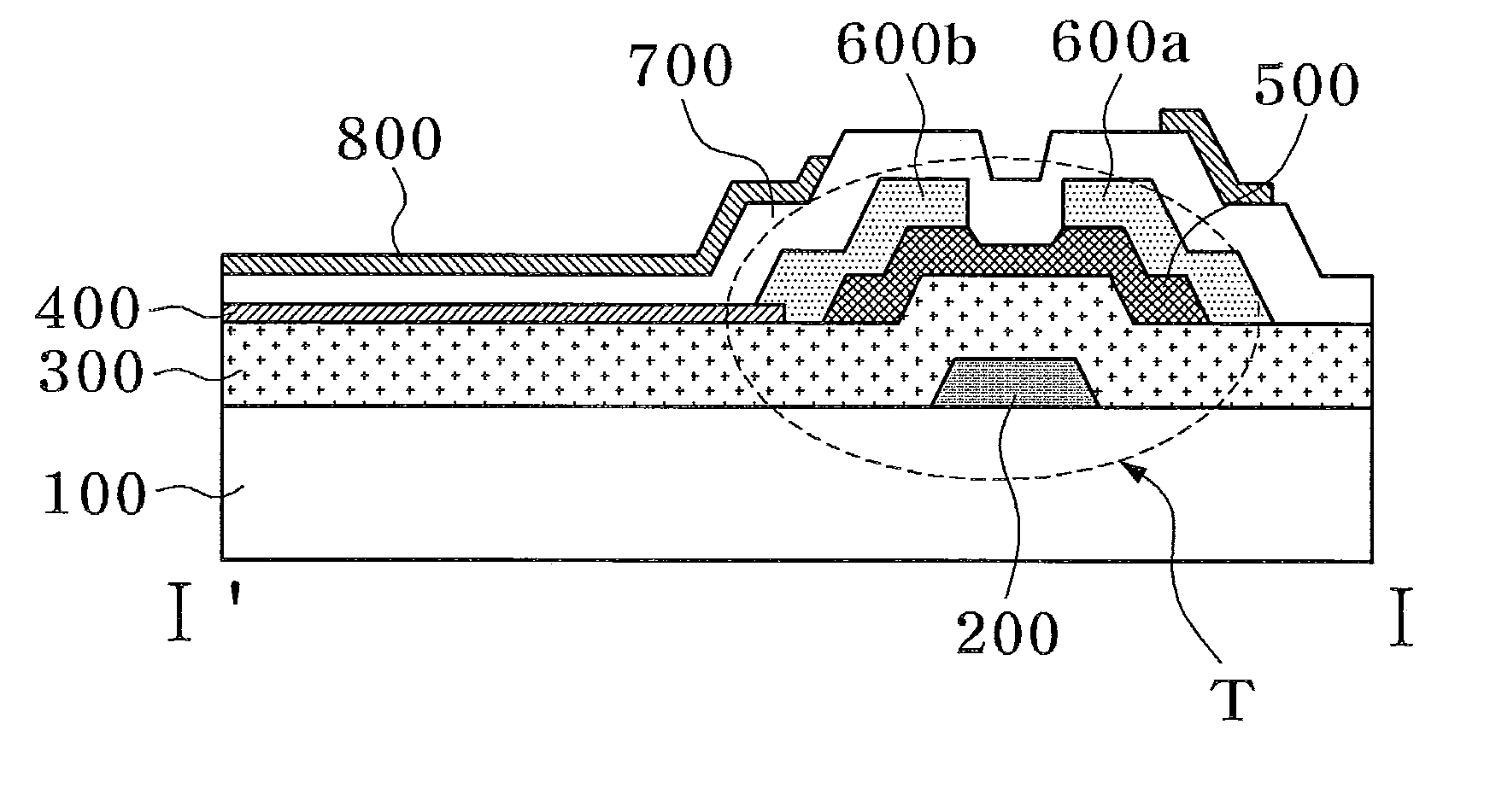
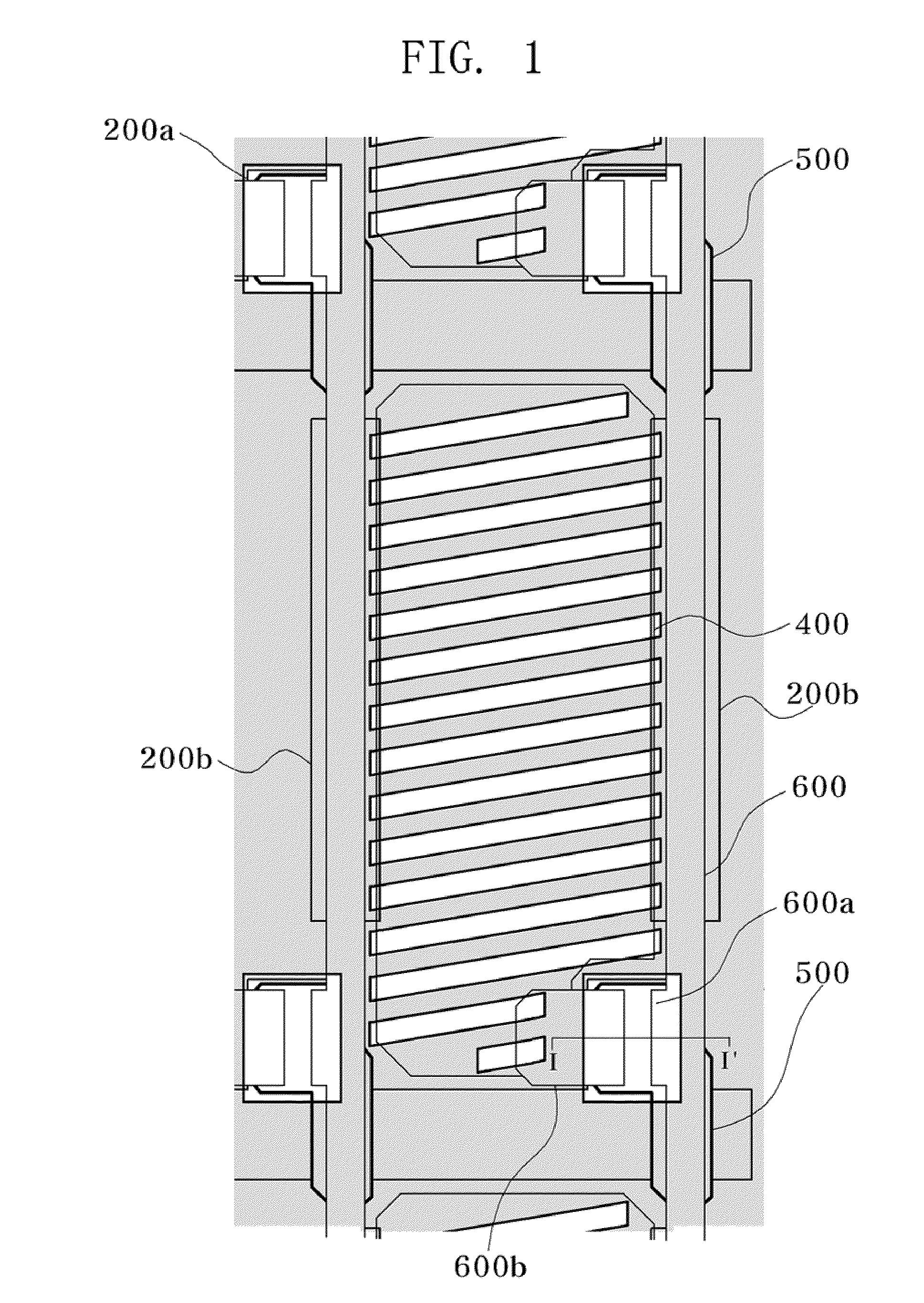
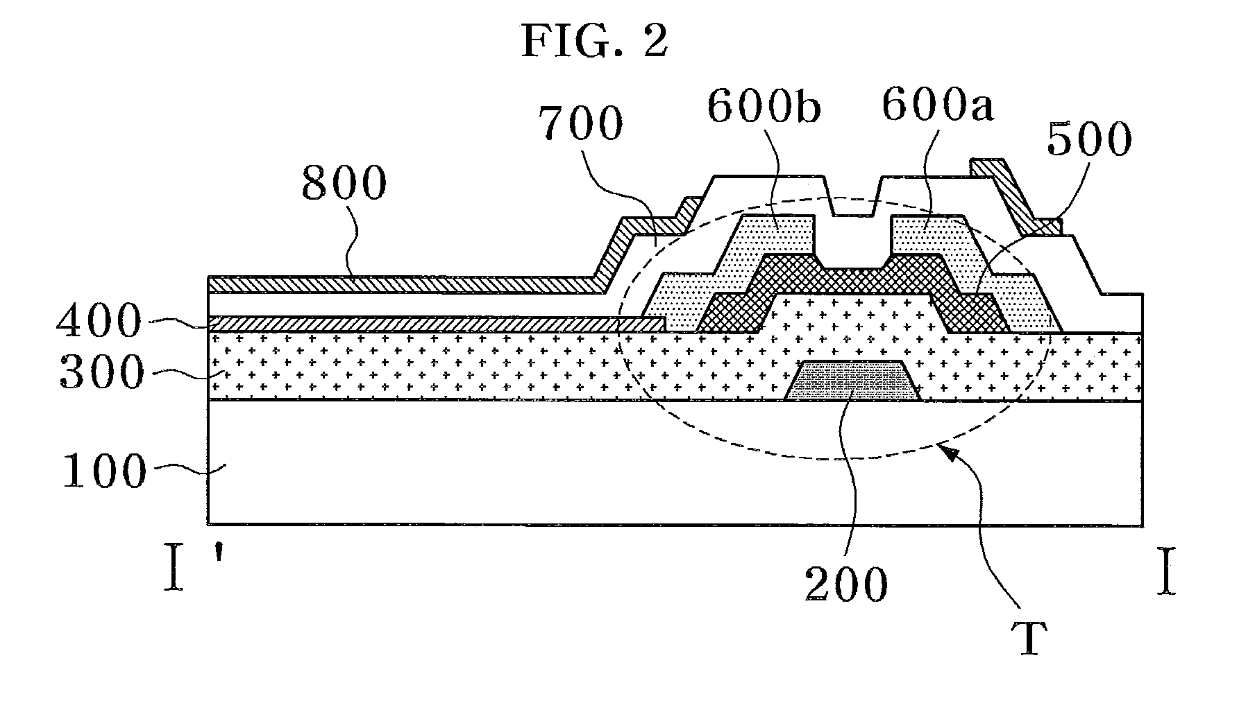
[0028]FIG. 1 is a plan view showing a portion of a pixel region formed at a lower substrate of an FFS mode LCD in accordance with an exemplary embodiment of the present invention, FIG. 2 is a cross-sectional view taken along line IT of FIG. 1, and FIGS. 3A ...


PUM

PropertyMeasurementUnit
angleaaaaaaaaaa
angleaaaaaaaaaa
angleaaaaaaaaaa

Abstract

Provided is a liquid crystal display including a transparent pixel electrode and a transparent common electrode in a pixel region to drive liquid crystals. The transparent common electrode includes a plurality of slits and is configured to open at least a portion of a switching device to connect unit pixels, the slits have an angle of 5 to 10° with respect to a gate line, and a rubbing direction of a liquid crystal layer is substantially parallel to a gate direction. Therefore, it is possible to provide the liquid crystal display capable of removing factors decreasing an aperture ratio, preventing light from leaking, and further improving internal reflection.

Description

CROSS-REFERENCE TO RELATED APPLICATION[0001]This application claims priority to and the benefit of Korean Patent Application No. 2009-109177, filed on Nov. 12, 2009, the disclosure of which is incorporated herein by reference in its entirety.BACKGROUND[0002]1. Field of the Invention[0003]The present invention relates to a liquid crystal display device (LCD) and a method of fabricating the same, and more particularly, to an LCD and a method of fabricating the same that are capable of removing factors decreasing an aperture ratio, preventing light from leaking, and further improving internal reflection.[0004]2. Discussion of Related Art[0005]In general, a fringe field switching (FFS) mode LCD has been proposed to improve a low aperture ratio and transmittance of an in-plane switching (IPS) mode LCD.[0006]The FFS mode LCD includes a common electrode (counter electrode) and a pixel electrode which are formed of a transparent conductive material to increase an aperture ratio and transmit...

Claims


Application Information

Patent Timeline
Patent Type & Authority Applications(United States)
IPC IPC(8): G02F1/1343H01L33/60
CPCG02F1/133707G02F2203/02G02F2001/134372G02F1/136209G02F1/134372G02F1/1343
Inventor SON, OCK SOOLEE, WON HEECHOI, SOO YOUNGSUH, DONG HAE
Owner HYDIS TECH
Why Eureka
Try Eureka