High-frequency circuit, high-frequency device, and communications apparatus

a high-frequency circuit and high-frequency technology, applied in waveguide-type devices, diversity/multi-antenna systems, digital transmission, etc., can solve the problems of complex circuit structure, high-frequency circuit, inability to handle multi-band wireless communications and mimo, etc., to suppress transmission power loss and high receiving sensitivity

Active Publication Date: 2011-05-12
MURATA MFG CO LTD
View PDF6 Cites 47 Cited by
  • Summary
  • Abstract
  • Description
  • Claims
  • Application Information

AI Technical Summary

Benefits of technology

[0006]Accordingly, an object of the present invention is to provide a high-frequency circuit and a high-frequency device capable of handling different communications systems with high receiving sensitivity and suppressed transmission power loss, and a communications apparatus comprising it.

Problems solved by technology

However, the high-frequency circuit described in WO 2006 / 003959 cannot handle a combination of multiband wireless communications and MIMO.
Also, because wireless communications systems of a MIMO system have an increased number of circuit structures such as receiving terminals, etc. for one communications system, isolation is difficult between pluralities of communications systems, resulting in complicated circuit structures.
Therefore, the use of the MIMO system in multiband wireless communications is extremely difficult.

Method used


Image

  • High-frequency circuit, high-frequency device, and communications apparatus
  • High-frequency circuit, high-frequency device, and communications apparatus
  • High-frequency circuit, high-frequency device, and communications apparatus

Examples


first embodiment

[0081](1) First embodiment

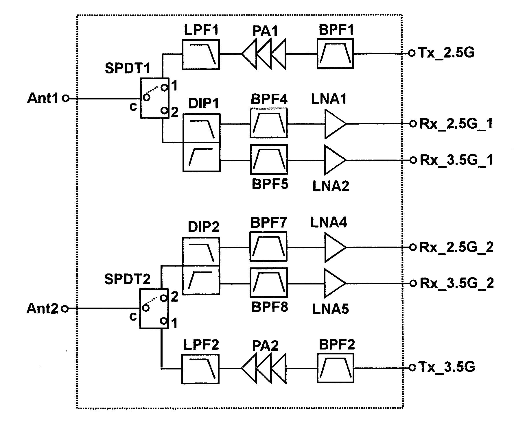
[0082]FIG. 1 shows one example of dual-band, high-frequency circuits using a 1T2R-type MIMO system. This high-frequency circuit comprises first and second antenna terminals Ant1, Ant2; a transmitting terminal Tx—2.5G, a first receiving terminal Rx—2.5G—1 and a second receiving terminal Rx—2.5G—2 for a first communications system; a transmitting terminal Tx—3.5G, a first receiving terminal Rx—3.5G—1 and a second receiving terminal Rx—3.5G—2 for a second communications system; and first and second switch circuits SPDT1, SPDT2 each having a common terminal c and first and second switching terminals 1, 2. Each of the first and second switch circuits SPDT1, SPDT2 is a single-pole, dual-throw-type switch circuit though not restrictive, and it may further comprise a switching terminal.

[0083]The first switch circuit SPDT1 comprises a common terminal c connected to a first antenna terminal Ant1, a first switching terminal 1 connected to the transmitting terminal Tx—...

second embodiment

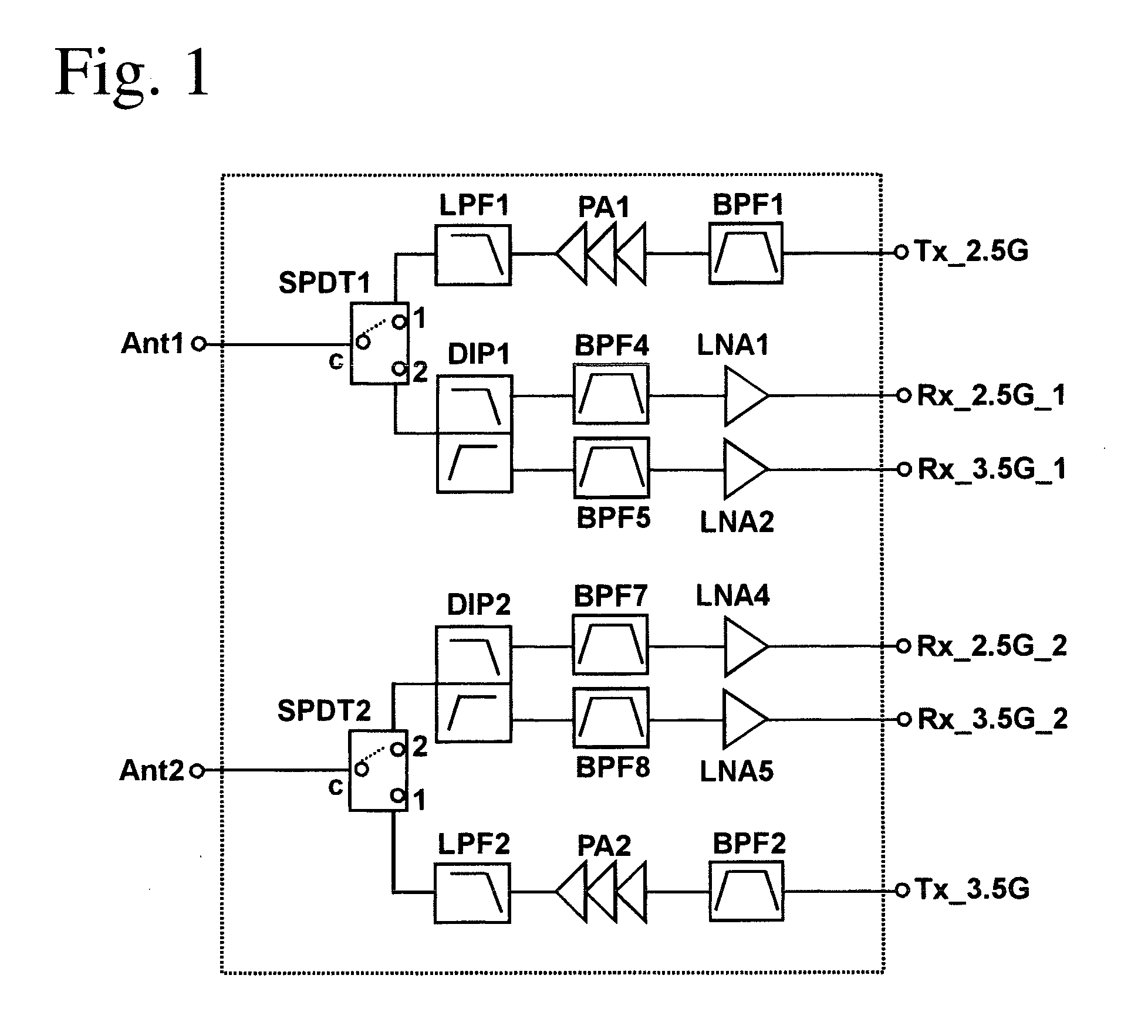
[0088](2) Second Embodiment

[0089]FIG. 2 shows another example of dual-band, high-frequency circuits using a 1T2R (one-transmission, two-reception)-type MIMO system. This high-frequency circuit differs from the high-frequency circuit according to the first embodiment, in the structures between the second switching terminal 2 of the first switch circuit SPDT1 and the first receiving terminal Rx—2.5G—1 for the first communications system and the first receiving terminal Rx—3.5G—1 for the second communications system, and in the structures between the second switching terminal 2 of the second switch circuit SPDT2 and the second receiving terminal Rx—2.5G—2 for the first communications system and the second receiving terminal Rx—3.5G—2 for the second communications system. Specifically, in the high-frequency circuit shown in FIG. 2, a low-noise amplifier circuit LNA11 is connected between the second switching terminal 2 of the first switch circuit SPDT1 and the first receiving-side multi...

third embodiment

[0091](3) Third Embodiment

[0092]FIG. 3 shows a still further example of dual-band, high-frequency circuits using a 1T2R (one-transmission, two-reception)-type MIMO system. In this high-frequency circuit, each of first and second switch circuits SP3T1, SP3T2 is a single-pole, triple-throw type having a common terminal and first to third switching terminals 1-3, the second and third switching terminals 2, 3 of the first switch circuit SP3T1 being connected to the first receiving terminal Rx—2.5G—1 for the first communications system and the first receiving terminal Rx—3.5G—1 for the second communications system, respectively, and the second and third switching terminals 2, 3 of the second switch circuit SP3T2 being connected to the second receiving terminal Rx—2.5G—2 for the first communications system and the second receiving terminal Rx—3.5G—2 for the second communications system, respectively. Namely, the first receiving terminal Rx—2.5G—1 for the first communications system and th...


PUM


Abstract

A high-frequency circuit comprising first and second antenna terminals, a transmitting terminal and first and second receiving terminals for first and second communications systems, and first and second switch circuits each having a common terminal and at least first and second switching terminals; the first antenna terminal being connected to a common terminal of the first switch circuit, the transmitting terminal for the first communications system being connected to the first switching terminal of the first switch circuit, the second antenna terminal being connected to a common terminal of the second switch circuit, the transmitting terminal for the second communications system being connected to the first switching terminal of the second switch circuit, each first receiving terminal for the first and second communications systems being connected to the second switching terminal of the first switch circuit via a first receiving-side multiplexer circuit, each second receiving terminal for the first and second communications systems being connected to the second switching terminal of the second switch circuit via a second receiving-side multiplexer circuit.

Description

FIELD OF THE INVENTION[0001]The present invention relates to a high-frequency circuit commonly usable in at least two different communications systems between electronic or electric equipments, a high-frequency device having such high-frequency circuit, and a communications apparatus comprising it.BACKGROUND OF THE INVENTION[0002]Data communications by wireless LAN such as IEEE802.11 are now widely used, for instance, in personal computers (PCs), PC peripherals such as printers, hard disk drives and broadband routers, electronic apparatuses such as FAXs, refrigerators, standard television sets (SDTVs), high-definition television sets (HDTVs), digital cameras, digital video cameras and mobile phones, signal-transmitting means in automobiles and aircrafts, etc.[0003]As the wireless LAN standard, IEEE802.11a uses an orthogonal frequency division multiplexing (OFDM) modulation system in a frequency band of 5 GHz, supporting high-speed data communications of maximum 54 Mbps. IEEE802.11b ...

Claims


Application Information

Patent Timeline
Patent Type & Authority Applications(United States)
IPC IPC(8): H04B7/02
CPCH01P1/20336H04B1/0057H01L2924/1461H01L2924/3025H01L2924/30107H01L2924/3011H01L2924/19105H01L2224/73265H01L2224/48227H01L2224/32225H04B1/48H01L2924/00012H01L2924/00H01L24/73
Inventor FUKAMACHI, KEISUKEKEMMOCHI, SHIGERU
Owner MURATA MFG CO LTD
Why Eureka
Try Eureka