Transistor

a transistor and transistor technology, applied in the field of transistors, can solve the problems of inability to recover the above changes in electrical properties in milliseconds, and the operation current change cannot be achieved in milliseconds, and achieve the effect of low photosensitivity and high electrical stability

Inactive Publication Date: 2011-05-19
IND TECH RES INST
View PDF17 Cites 2 Cited by
  • Summary
  • Abstract
  • Description
  • Claims
  • Application Information

AI Technical Summary

Benefits of technology

[0008]The invention is directed to a transistor having high electrical stability and low photosensitivity.

Problems solved by technology

However, the transistor is highly photosensitive; that is, when the light irradiates the transistor, the electrical property of the transistor is affected immediately, so as to result in electrical drift phenomenon such as threshold voltage shift, sub-threshold swing increase, operating current change, and so on.
In addition, the above changes in electrical property cannot be recovered in milliseconds.

Method used


Image

  • Transistor
  • Transistor
  • Transistor

Examples


first embodiment

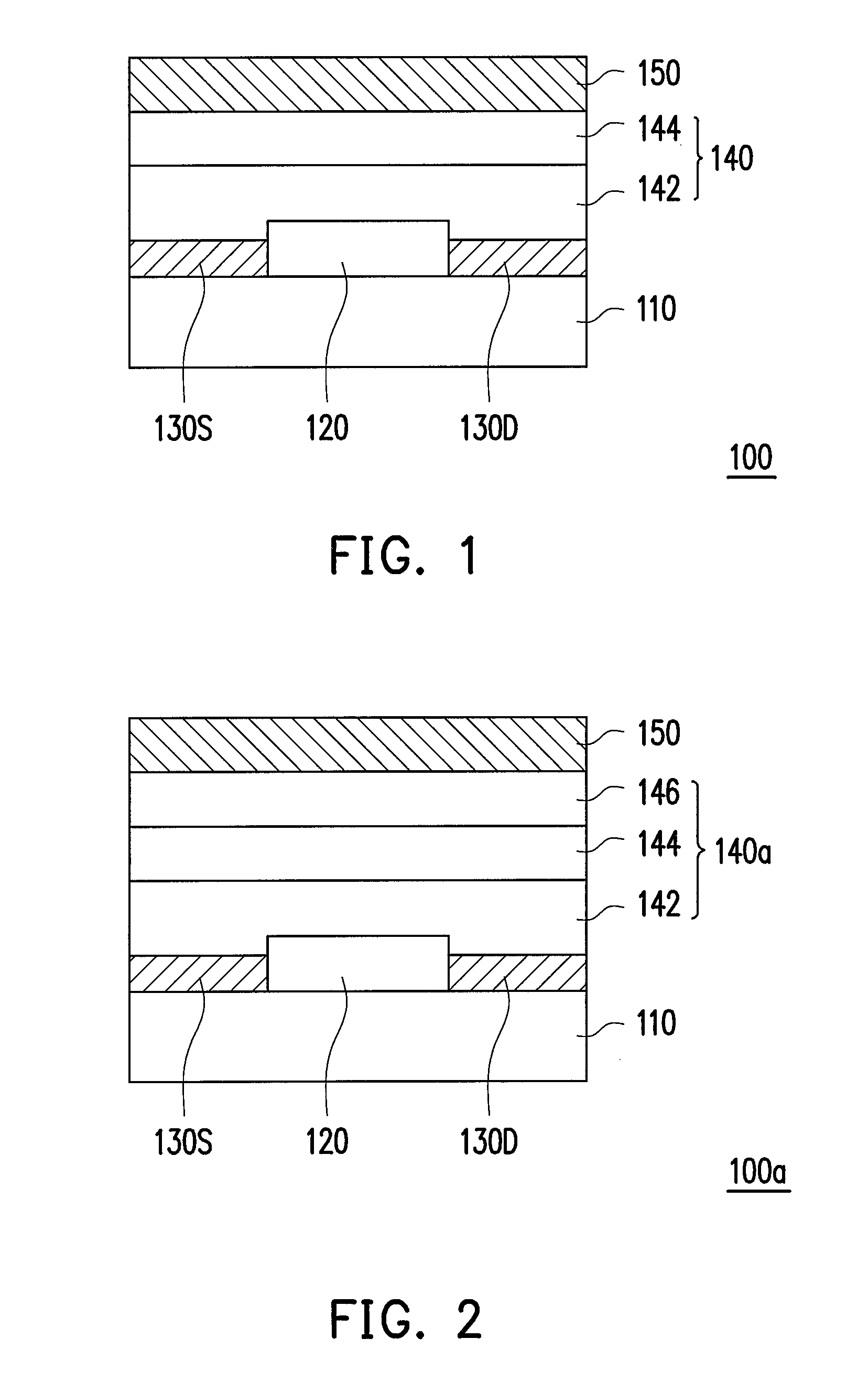
[0020]FIG. 1 is a schematic cross-sectional view of a transistor according to a first embodiment of the invention.

[0021]Referring to FIG. 1, a transistor 100 includes a substrate 110, a semiconductor layer 120, a source 130S and a drain 130D, a stacked insulating layer 140, and a gate 150. The semiconductor layer 120 is disposed on the substrate 110 and adopts a first type carrier as the main carrier. The source 130S and the drain 130D are disposed on the substrate 110 and at two sides of the semiconductor layer 120. Specifically, in the present embodiment, the first type carrier is a hole; that is, the semiconductor layer 120 is a P-type semiconductor layer having more holes, for example. The semiconductor layer 120 is made of inorganic semiconductor or organic semiconductor. Here, inorganic semiconductor includes amorphous silicon, polysilicon, or oxide semiconductors, and organic semiconductor includes organic small molecules, organic polymers, or a mixture thereof. Moreover, the...

second embodiment

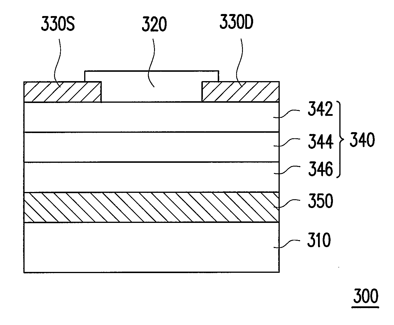
[0027]FIG. 2 is a schematic cross-sectional view of a transistor according to a second embodiment of the invention. A transistor 100a of the present embodiment and the transistor 100 of FIG. 1 have similar structures; however, the main difference is that the transistor 100a further includes a third insulating layer 146. Thus, only the different parts are described hereinafter.

[0028]Referring to FIG. 2, the transistor 100a includes the substrate 110, the semiconductor layer 120, the source 130S and the drain 130D, a stacked insulating layer 140a, and the gate 150. The stacked insulating layer 140a includes the first insulating layer 142, the second insulating layer 144, and the third insulating layer 146 stacked sequentially on the semiconductor layer 120. In the present embodiment, the semiconductor layer 120 adopts holes as the main carrier, and is, for example, a P-type semiconductor layer. The first insulating layer 142, for example, contains the first group which withdraws holes...

third embodiment

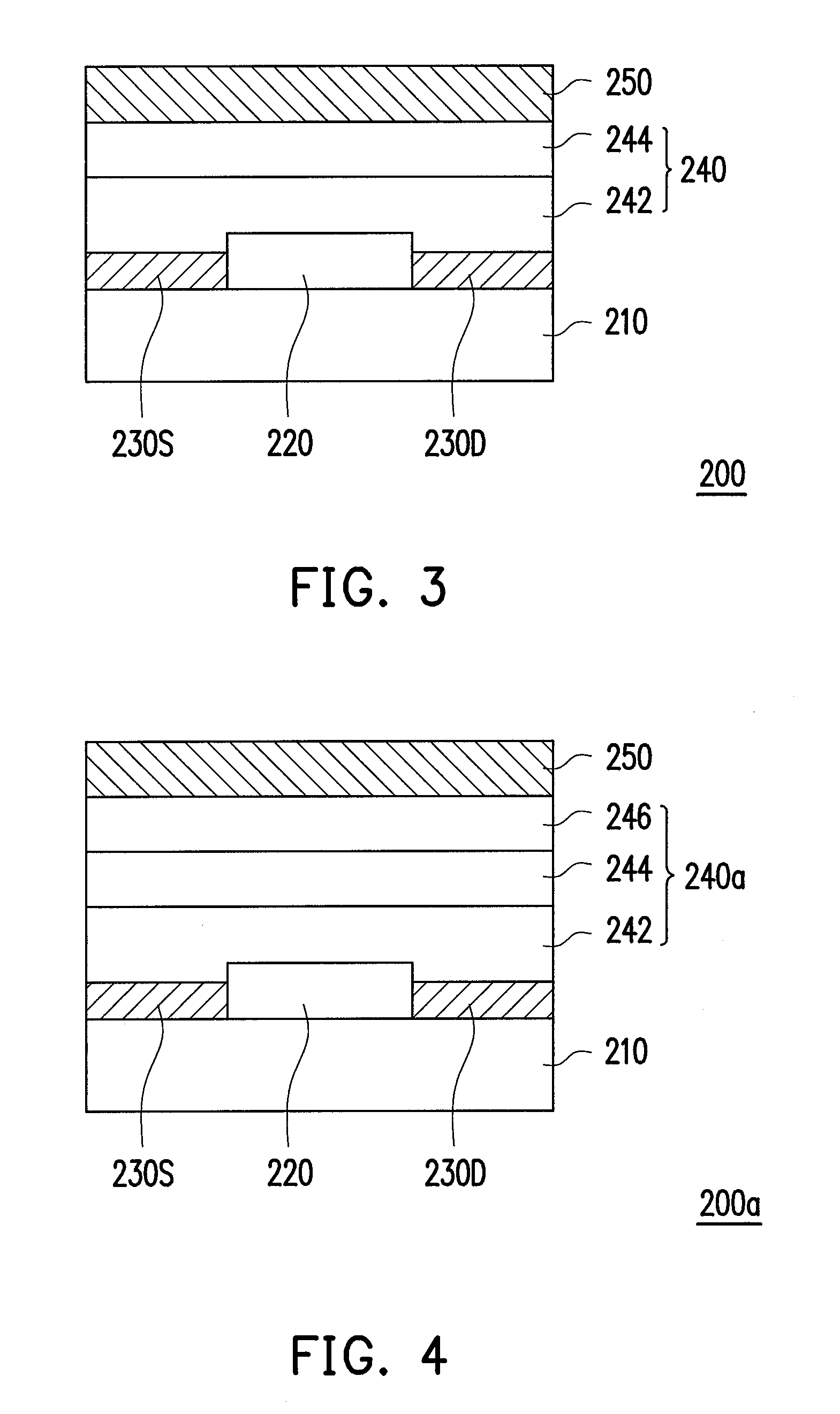
[0032]FIG. 3 is a schematic cross-sectional view of a transistor according to a third embodiment of the invention. A transistor 200 of the present embodiment and the transistor 100 of FIG. 1 have similar structures; however, the main difference is that the semiconductor layer 220 of the transistor 200 adopts electrons as the main carrier. Thus, only the different parts are described hereinafter.

[0033]Referring to FIG. 3, a transistor 200 includes a substrate 210, a semiconductor layer 220, a source 230S and a drain 230D, a stacked insulating layer 240, and a gate 250. The semiconductor layer 220 is disposed on the substrate 210 and adopts electrons as the main carrier. The gate 250 is disposed on the substrate 210. The stacked insulating layer 240 is disposed between the semiconductor layer 220 and the gate 250, and includes a first insulating layer 242 and a second insulating layer 244. Herein, the first insulating layer 242 contains a group which withdraws electrons, the second in...


PUM


Abstract

A transistor including a substrate, a gate, a semiconductor layer, a stacked insulating layer and a source and a drain is provided. The gate is disposed on the substrate. The semiconductor layer is disposed on the substrate, and a first type carrier is the main carrier in the semiconductor layer. The stacked insulating layer is disposed between the semiconductor layer and the gate, and includes a first insulating layer and a second insulating layer. The first insulating layer contains a first group withdrawing the first type carrier, the second insulating layer contains a second group withdrawing a second type carrier, and the first insulating layer is disposed between the semiconductor layer and the second insulating layer. The source and the drain are disposed on the substrate and at two sides of the semiconductor layer.

Description

CROSS-REFERENCE TO RELATED APPLICATION[0001]This application claims the priority benefit of Taiwan application serial no. 98139338, filed on Nov. 19, 2009. The entirety of the above-mentioned patent application is hereby incorporated by reference herein and made a part of specification.BACKGROUND OF THE INVENTION[0002]1. Field of the Invention[0003]The invention relates to a semiconductor device, and more particularly, to a transistor.[0004]2. Description of Related Art[0005]The transistor plays a role of driving the display medium in the display, and in the process of driving the display medium, the stability of the electrical property of the transistor affects the image contrast displayed by the display medium. Thus, for the display to have superior display quality, the transistor array has to maintain stable threshold voltage and operating current.[0006]Generally, the transistor has stable threshold voltage and operating current in an environment that is dark and lacks moisture a...

Claims


Application Information

Patent Timeline
Patent Type & Authority Applications(United States)
IPC IPC(8): H01L29/792
CPCH01L51/0533H01L29/4908H10K10/476
Inventor LO, PO-YUANPENG, YU-RUNGHU, TARNG-SHIANGCHAN, YI-JEN
Owner IND TECH RES INST
Why Eureka
Try Eureka