Field-effect transistor and manufacturing process thereof

Active Publication Date: 2013-10-17
GEORGIA TECH RES CORP
View PDF6 Cites 26 Cited by
  • Summary
  • Abstract
  • Description
  • Claims
  • Application Information

AI Technical Summary

Benefits of technology

[0009]The object of the invention is to provide a FET having high electrical stability that at the same time can operate at low vol

Problems solved by technology

The most common sign of device degradation manifests itself as a threshold voltage shift upon prolonged gate bias stress.
However, polymers have typically a very low

Method used


Image

  • Field-effect transistor and manufacturing process thereof
  • Field-effect transistor and manufacturing process thereof
  • Field-effect transistor and manufacturing process thereof

Examples


Example

Example 1

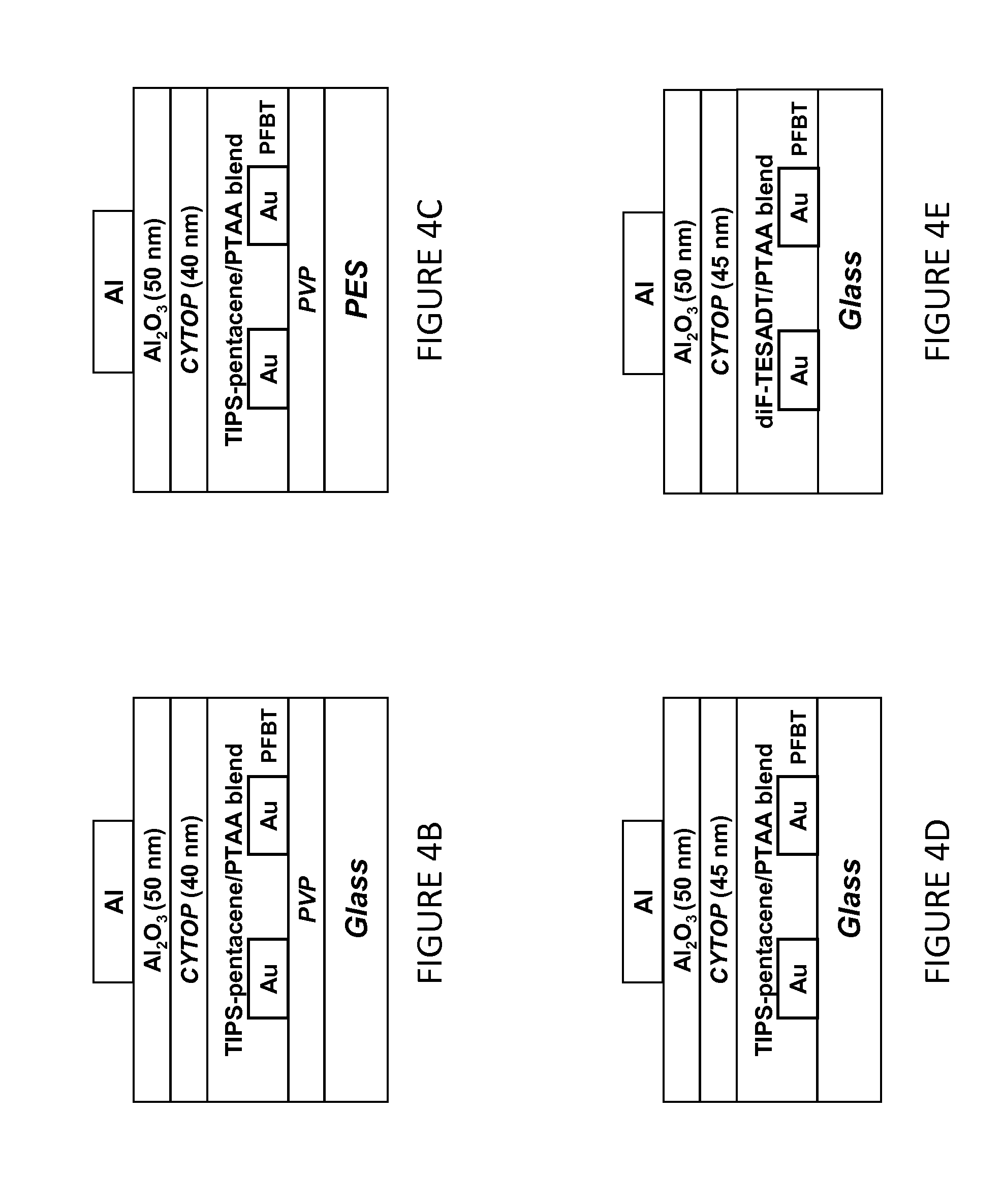
TIPS-Pentacene and Poly (Triarylamine) (PTAA) Blend Channel Based OFET with CYTOP / Al2O3 Bi-Layer Using Glass Substrate (40 nm CYTOP; 50 nm Al2O3)

[0094]OFETs with a bottom-contact and top-gate structure were fabricated on glass substrates (Corning 1737). Poly-4-vinylphenol (PVP) buffer layers were prepared from 2 wt. % solutions of PVP (Mw˜20,000) and poly (melamine-co-formaldehyde), as a cross-linking agent, in propylene glycol monomethyl ether acetate (PGMEA), which were deposited by spin coating at 3000 rpm for 40 sec and subsequently cross-linked at 175° C. on a hot plate for 1 h in a N2-filled glove box. Au (50 nm) bottom-contact source / drain electrodes were deposited by thermal evaporation through a shadow mask. A self-assembled monolayer of pentafluorobenzenethiol (PFBT) was formed on the Au electrodes by immersion in a 10 mmol PFBT solution in ethanol for 15 min in a N2-filled dry box, rinsing with pure ethanol, and drying. The TIPS-pentacene and PTAA blend solution ...

Example

Example 2

Pentacene Channel Based OFET

[0095]The top gate pentacene OFETs were fabricated with a geometry incorporating a bottom source / drain electrodes. Au (80 nm) bottom contact source / drain electrodes were deposited by electron-beam (e-beam) at room temperature on a glass substrate through a shadow mask. A pentacene active layer (50 nm) was then deposited by thermal evaporation at room temperature through a shadow mask. CYTOP (40 nm) / Al2O3 (50 nm) layers were used as a top gate dielectric. CYTOP (40 nm) layers were coated by spin casting at 3000 rpm for 60 seconds. The CYTOP films were annealed at 100° C. for 20 min. Al2O3 dielectric films were grown at 110° C. using alternating exposures of trimethyl aluminum [Al(CH3)3] and H2O vapor at a deposition rate of approximately 0.1 nm per cycle. Then, Al electrode was sequentially deposited by e-beam to form the gate electrode.

Example

Example 3

InGaZnO Channel Based Oxide FET

[0096]The top gate amorphous InGaZnO FET was fabricated with a geometry incorporating a bottom source / drain electrodes. First, a tri-layer of Ti (6 nm) / Au (50 nm) / Ti (6 nm) was deposited using electron-beam (e-beam) at room temperature on a glass substrate (Corning 1737) and patterned by photolithography followed by a lift-off process. A 40 nm-thick a-IGZO (Ga2O3:In2O3:ZnO=1:1:2 mol %) active layer was then deposited by radio frequency (RF) sputtering. After deposition of the a-IGZO layer, the device was annealed. To define the channel, the a-IGZO layer was patterned by a wet-etching process using hydrochloric acid (HCl:H2O=1:100) diluted in DI water. CYTOP (40 nm) / Al2O3 (50 nm) layers were used as top gate dielectrics. Al2O3 dielectric films were grown at 110° C. using alternating exposures of trimethyl aluminum [Al(CH3)3] and H2O vapor. For 40 nm CYTOP layer, a 2 wt % solution was used, which was diluted with solvent. CYTOP (40 nm) layers we...


PUM


Abstract

A field-effect transistor includes a gate, a source and a drain; a semiconductor layer between the source and the drain; and a gate insulator between the gate and the semiconductor layer. The gate insulator comprises a first layer adjoining the semiconductor layer; and a second layer. The first layer is formed from an amorphous fluoropolymer having a first dielectric constant and a first thickness. The second layer has a second dielectric constant and a second thickness. The first dielectric constant is smaller than 3, the first thickness is smaller than 200 nm, the second dielectric constant is higher than 5, and the second thickness is smaller than 500 nm.

Description

STATEMENT OF GOVERNMENT LICENSE RIGHTS[0001]The inventors received partial funding support through the STC Program of the National Science Foundation under Agreement Number DMR-0120967 and the Office of Naval Research through Contract Award Number N00014-04-1-0120. The Federal Government has certain license rights in this invention.BACKGROUND[0002]1. Field of the Invention[0003]The present invention relates to a field-effect transistor, a manufacturing process thereof and a circuit comprising a plurality of such transistors.[0004]2. Description of the Related Art[0005]Over the last several years, organic and mixed transition metal oxide semiconductor channel based field-effect transistors (FETs) have been extensively studied because they can potentially lead to low-end consumer electronic applications that can be produced at a very low cost on large areas, and on flexible or free-form substrates.[0006]Two critical aspects for the realization of these technologies relate to: 1) the e...

Claims


Application Information

Patent Timeline
IPC IPC(8): H01L51/05
CPCH01L51/0529H01L27/1225H10K85/621H10K85/657H10K10/476H10K10/466C07D471/06H10K10/00H10K10/474
Inventor HWANG, DO KYUNGKIM, JUNGBAEFUENTES-HERNANDEZ, CANEKKIPPELEN, BERNARD
Owner GEORGIA TECH RES CORP
Why Eureka
Try Eureka