Photoresist coating and developing apparatus, substrate transfer method and interface apparatus

a technology of developing apparatus and coating, applied in the direction of photomechanical apparatus, instruments, photosensitive materials, etc., can solve the problems of large reduction of deviation of the alignment of patterns, and inability to control the temperature of the photoresist coating and developing apparatus, so as to reduce the change in the temperature of the wafer

Active Publication Date: 2011-05-19
TOKYO ELECTRON LTD
View PDF2 Cites 253 Cited by
  • Summary
  • Abstract
  • Description
  • Claims
  • Application Information

AI Technical Summary

Benefits of technology

[0015]In accordance with an embodiment of the present disclosure, there are provided a photoresist coating and developing apparatus, a photoresist coating and developing method and an interface...

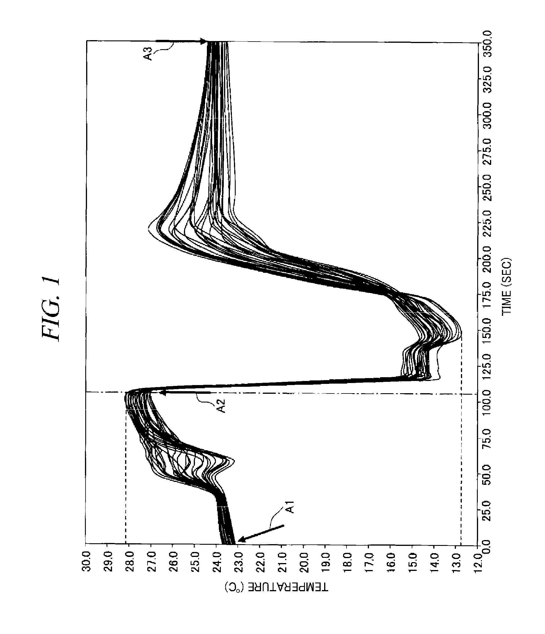
Problems solved by technology

However, when photoresist patterns each having a line width of about 20 nm or less are formed through an exposure process, alignment of patterns may be deviated due to thermal expansion of a wafer.
As a result of the examination, it has been found that even if the temperature of the wafer is precisely controlled in the photoresist coating and developing apparatus, the temperature of the wafer is greatly decrea...

Method used


Image

  • Photoresist coating and developing apparatus, substrate transfer method and interface apparatus
  • Photoresist coating and developing apparatus, substrate transfer method and interface apparatus
  • Photoresist coating and developing apparatus, substrate transfer method and interface apparatus

Examples


Embodiment Construction

[0023]Hereinafter, non-limiting embodiments of the present disclosure will be explained in detail with reference to accompanying drawings. In the whole drawings, same or corresponding elements or parts are assigned same or corresponding reference numerals and redundant description thereof may be omitted.

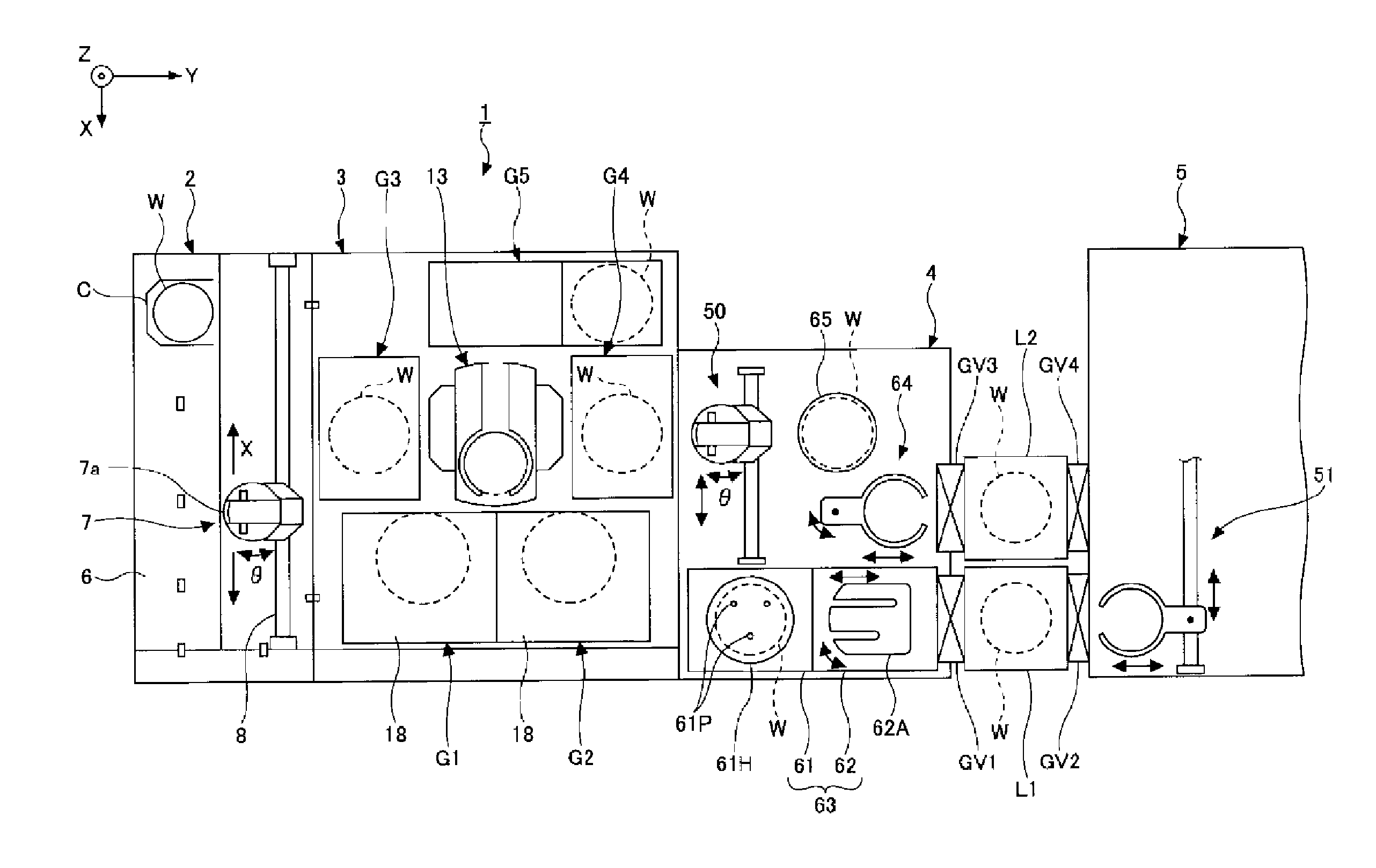
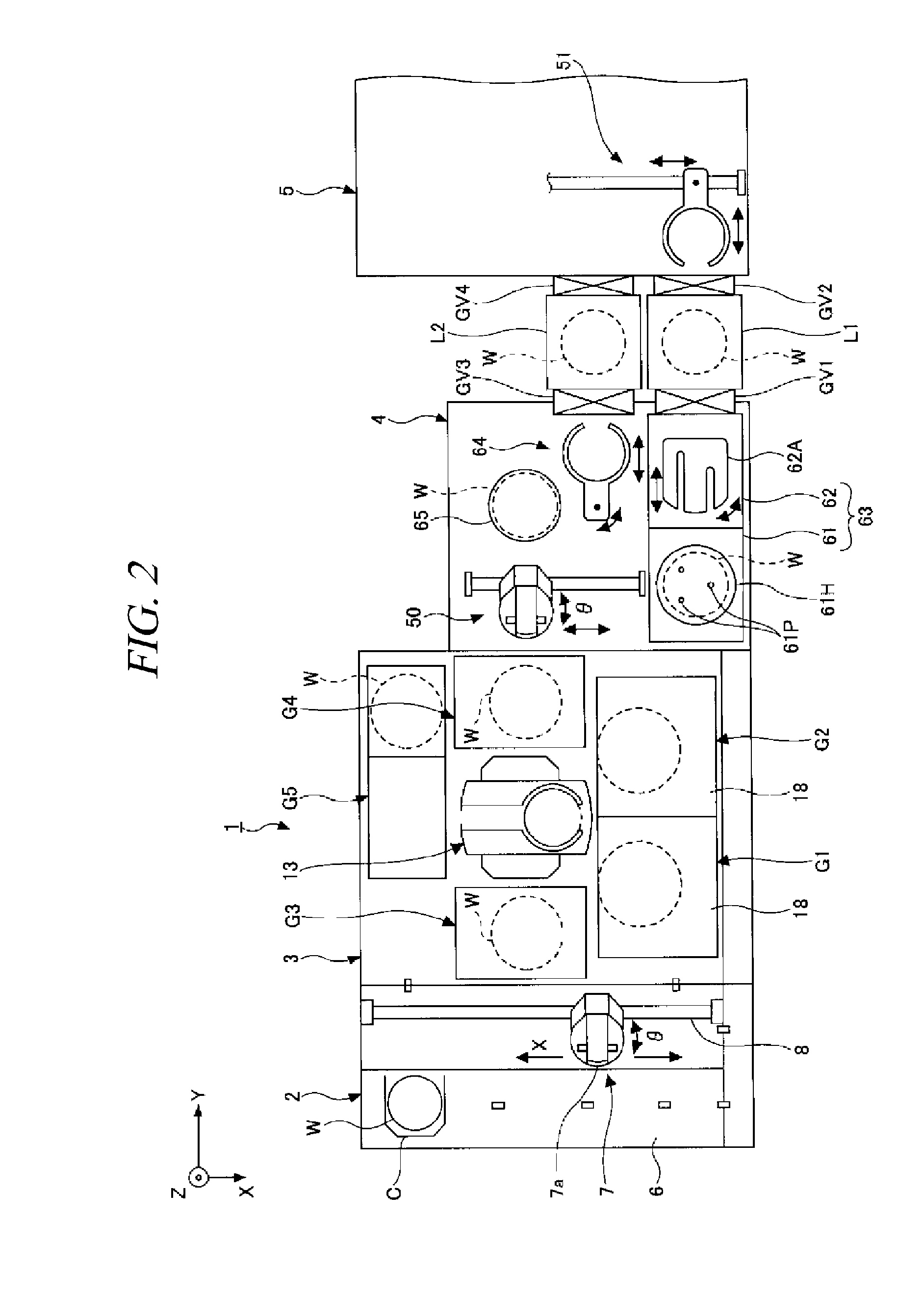
[0024]FIG. 2 is a plane view schematically showing a configuration of a photoresist coating and developing apparatus 1 in accordance with an embodiment of the present disclosure, FIG. 3 is a front view schematically showing the photoresist coating and developing apparatus 1, and FIG. 4 is a rear view schematically showing the photoresist coating and developing apparatus 1.

[0025]As depicted in FIG. 2, the photoresist coating and developing apparatus 1 includes a cassette station 2, a processing station 3, and an interface apparatus 4.

[0026]The cassette station 2 includes a mounting table 6 on which a cassette C accommodating, for example, about 25 sheets of wafers W is mounted; and a ...


PUM

PropertyMeasurementUnit
Temperatureaaaaaaaaaa

Abstract

A photoresist coating and developing apparatus 1 includes a photoresist film forming unit that forms a photoresist film on a substrate; a heat treatment unit that heats the substrate on which the photoresist film is formed by the photoresist film forming unit; a cooling unit that cools the substrate, on which the photoresist film is formed and which is heated by the heat treatment unit, to normal temperature; a heating unit 61 that heats the substrate, which is cooled to normal temperature by the cooling unit, to a predetermined temperature; a load-lock chamber L1 that unloads the substrate under depressurized atmosphere to expose the photoresist film; and a transfer device 62 that transfers the substrate from the heating unit 61 to the load-lock chamber L1.

Description

CROSS-REFERENCE TO RELATED APPLICATION[0001]This application claims the benefit of Japanese Patent Application No. 2009-259872 filed on Nov. 13, 2009, the entire disclosures of which are incorporated herein by reference.FIELD OF THE INVENTION[0002]The present disclosure relates to a photoresist coating and developing apparatus which forms a photoresist film on a substrate and develops the photoresist film exposed by an exposure apparatus. In particular, the present disclosure relates to a photoresist coating and developing apparatus suitable to be used with an exposure apparatus that exposes a photoresist film under vacuum and a substrate transfer method in this photoresist coating and developing apparatus.BACKGROUND OF THE INVENTION[0003]As a semiconductor device has been getting miniaturized, a line width is required to be about 20 nm or less. In order to get such a line width, development of an extreme ultraviolet light (hereinafter, referred to as “EUV light”) exposure apparatus...

Claims


Application Information

Patent Timeline
IPC IPC(8): G03F7/004C23C14/00
CPCH01L21/67109H01L21/67201H01L21/67196G03F7/202G03F7/70891H01L21/0274H01L21/681
Inventor YAMADA, YOSHIAKIYAMAMOTO, YUICHIKOSUGI, HITOSHI
Owner TOKYO ELECTRON LTD
Why Eureka
Try Eureka