Control and readout of electron or hole spin

a technology of electron or hole spin and control, applied in the direction of superconductor devices, instruments, and details of semiconductor/solid-state devices, can solve the problem of reducing the vulnerability of devices

Active Publication Date: 2011-05-26
NEWSOUTH INNOVATIONS PTY LTD
View PDF14 Cites 39 Cited by
  • Summary
  • Abstract
  • Description
  • Claims
  • Application Information

AI Technical Summary

Benefits of technology

[0025]Besides its compactness and elegance, the proposed structure is truly innovative in the idea of using the SET island to provide a charge reservoir for spin detection. The concept of combining the charge reservoir, local ESR and charge sensor in a single MOS device clearly constitutes a great advantage in flexibility for the layout of a planar structure for scalable quantum computing.
[0028]Additionally, the capability to control the qubit (electron or hole spin) by local ESR means that it is not necessary to Stark-shift the individual dopants to select which one is in resonance with a global microwave field. Therefore, the “A-gates” that were necessary in previously proposed architectures [15], could potentially be eliminated.

Problems solved by technology

Second, the thin (and nontunable) Al2O3 tunnel junctions—are replaced by tuneable barriers controlled by the gate potentials; this also reduces the vulnerability of the device due to uncontrolled or random electrostatic charges.

Method used


Image

  • Control and readout of electron or hole spin
  • Control and readout of electron or hole spin
  • Control and readout of electron or hole spin

Examples


Embodiment Construction

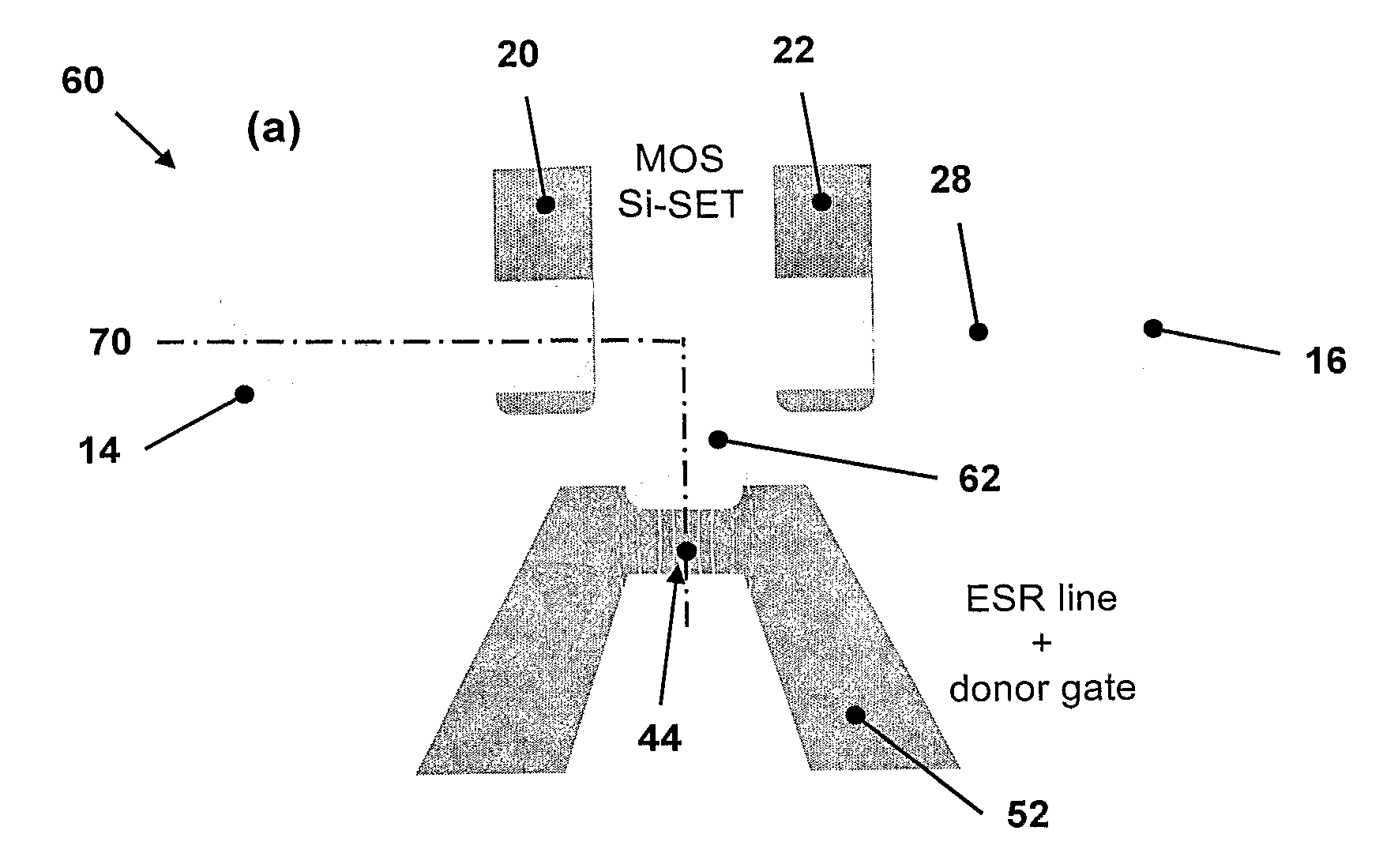
[0062]Referring now to FIG. 4(a) which shows a complete device 60 for control and readout of the electron or hole spin of a single dopant; remembering that a qubit can be realised in the electron or hole spin of a single dopant atom in silicon. There are a number of techniques available for inserting single donors, for instance those described in U.S. Pat. No. 7,176,066 and U.S. Pat. No. 7,061,008 to the applicant.

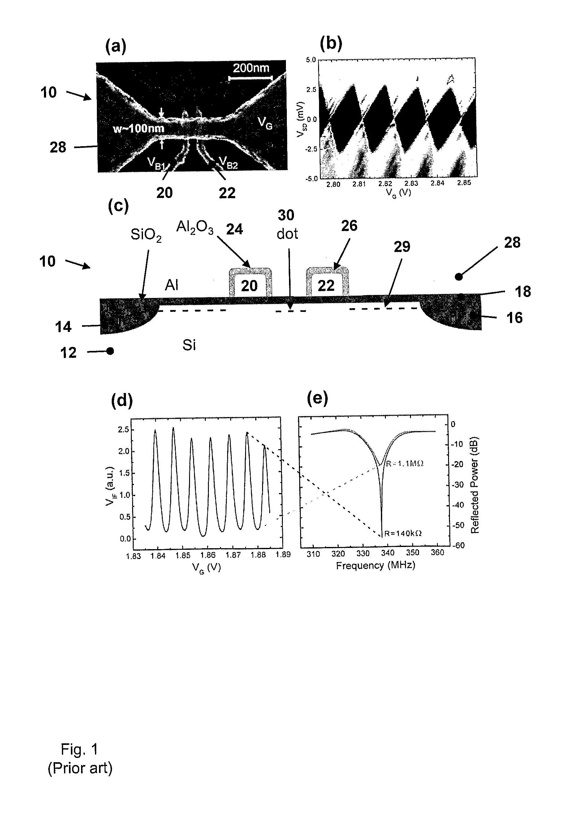
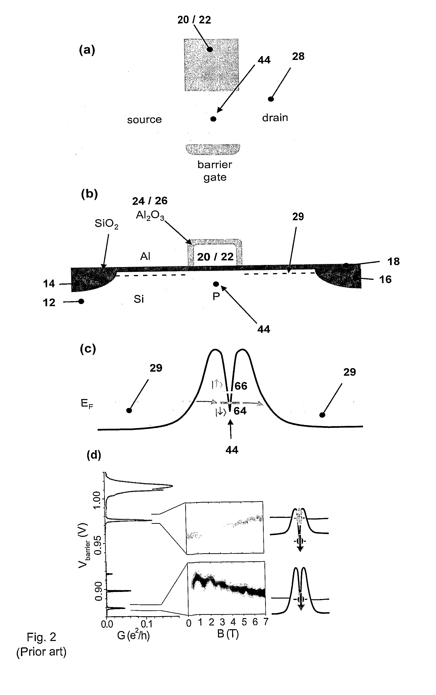
[0063]The device comprises a Si-SET as shown in FIG. 1(a) and (c), for single-shot detection of charge transfers between an individually placed dopant and a reservoir. In this case the dopant site 44 is in front of the Si-SET island. Also, the top gate 28 has an extended island 62 that protrudes towards the dopant site 44. As a result the GICL 30 in the SET is brought close enough to the implanted dopant 44 to allow (spin-dependent) charge tunnelling between them. The SET island 30 itself is acting as a reservoir for the spin-dependent charge tunnelling to and from the dop...


PUM


Abstract

This invention concerns an electronic device for the control and readout of the electron or hole spin of a single dopant in silicon. The device comprises a silicon substrate in which there are one or more ohmic contact regions. An insulating region on top of the substrate. First and second barrier gates spaced apart to isolate a small region of charges to form an island of a Single Electron Transistor (SET). A third gate over-lying both the first and second barrier gates, but insulated from them, the third gate being able to generate a gate-induced charge layer (GICL) in the ESR line substrate beneath it. A fourth gate in close proximity to a single dopant donor gate atom, the dopant atom being encapsulated in the substrate outside the region of the GICL but close enough to allow spin-dependent charge tunnelling between the dopant atom and the SET island under the control of gate potentials, mainly the fourth gate. In use either the third or fourth gate also serve as an Electron Spin Resonance (ESR) line to control the spin of the single electron or hole of the dopant atom. In a further aspect it concerns a method for using the device.

Description

TECHNICAL FIELD[0001]This invention concerns an electronic device for the control and readout of the electron or hole spin of a single dopant in silicon. In a further aspect it concerns a method for using the device.BACKGROUND ART[0002]On the roadmap towards building a scalable, silicon-based quantum computer, several essential milestones have already been achieved. Most importantly: The development of a single-ion implantation technology that allows the precise placement of individual phosphorus atoms in silicon [1]; The application of advanced nanofabrication, microwave and low-temperature techniques to the production and characterization of Single Electron Transistors (rf-SETs), with a charge sensitivity close to the quantum limit [2]; The control and detection of single electron transfers between individual phosphorus donors [3], obtained by combining the single-ion implantation and SET techniques; and, The layout of quantum device structures for universal fault-tolerant quantum...

Claims


Application Information

Patent Timeline
Patent Type & Authority Applications(United States)
IPC IPC(8): H03H11/24H01L29/775G06N99/00
CPCB82Y10/00G01N24/10H01L29/7613H01L29/66984G06N99/002G06N10/00
Inventor MORELLO, ANDREADZURAK, ANDREWHUEBL, HANS-GREGORCLARK, ROBERT GRAHAMWILLEMS VAN BEVEREN, LAURENS HENRYHOLLENBERG, LLOYD CHRISTOPHER LEONARDJAMIESON, DAVID NORMALESCOTT, CHRISTOPHER
Owner NEWSOUTH INNOVATIONS PTY LTD
Why Eureka
Try Eureka