Thin film silicon solar cell and manufacturing method thereof

a solar cell and thin film technology, applied in the direction of basic electric elements, electrical equipment, semiconductor devices, etc., can solve the problems of limiting the overall cell performance, recombination loss, and high recombination loss at the interface between the p-type window layer and the i-type absorber layer

Inactive Publication Date: 2011-06-02
KISCO CORP (KR)
View PDF6 Cites 9 Cited by
  • Summary
  • Abstract
  • Description
  • Claims
  • Application Information

AI Technical Summary

Problems solved by technology

However, an abrupt optical band gap difference at hetero-junction interface between the p-type window layer and the i-type absorber layer increases a defect density at the interface, and thereby causing recombination loss.
Further, if carbon is introduced to the p-type window layer to enhance the optical band gap,. it limits the overall cell performance due to a high series resistance.
However, because a graded band gap i-a-SiC:H buffer layer deposited without hydrogenated dilution has a large dangling bond defect density, recombination loss at the interface between the p-type window layer and the i-type absorber layer is still high.
Further, the graded band gap i-a-SiC:H buffer layer has a disadvantage that efficiency of a solar cell is reduced due to a low electric conductivity thereof.
Thus, it takes long time to produce the solar cell.
Accordingly, the photo-CVD method is not suitable for mass production of the solar cell.

Method used


Image

  • Thin film silicon solar cell and manufacturing method thereof
  • Thin film silicon solar cell and manufacturing method thereof
  • Thin film silicon solar cell and manufacturing method thereof

Examples


Embodiment Construction

[0031]The present embodiments will be described in detail with reference to accompanying drawings.

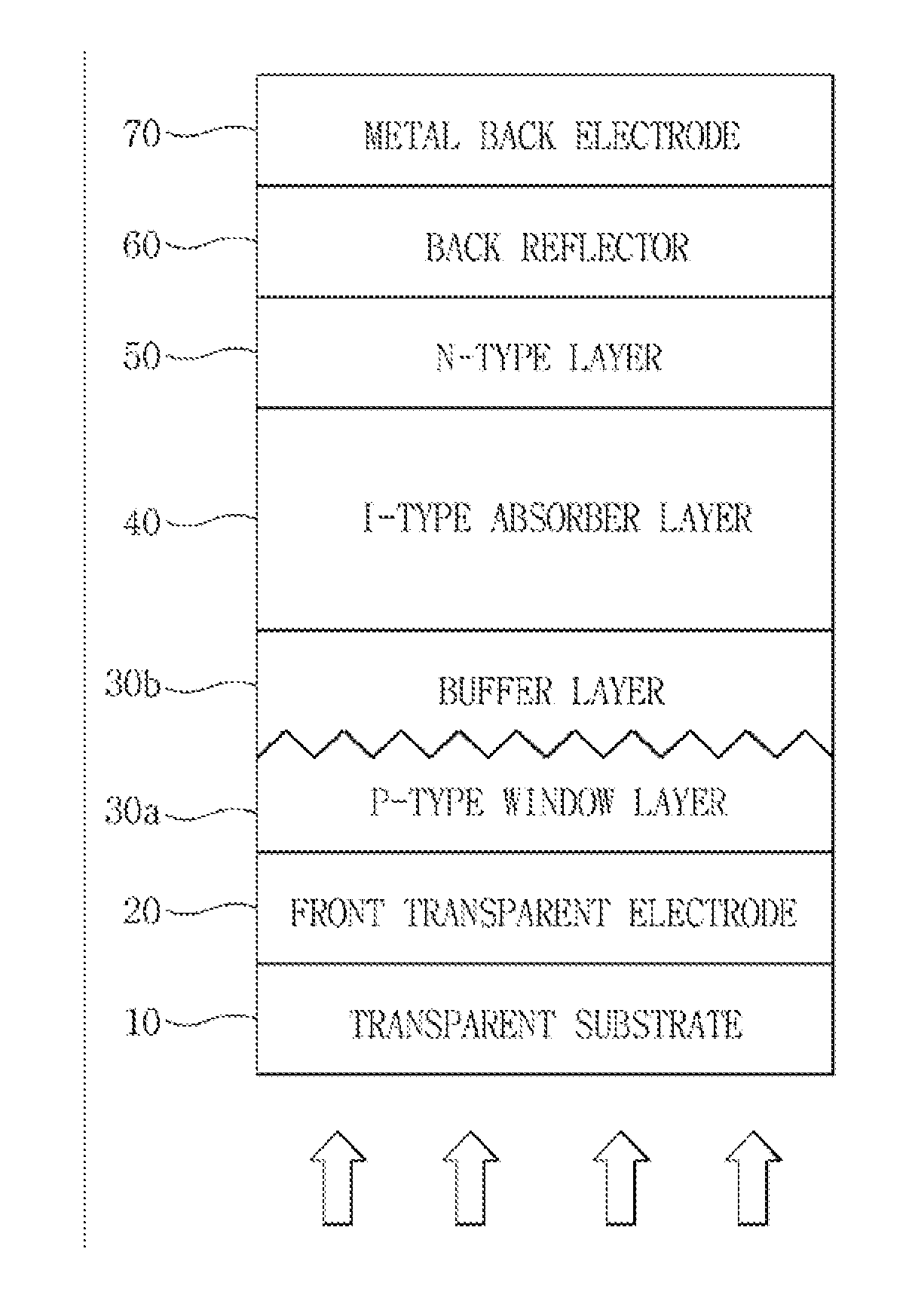
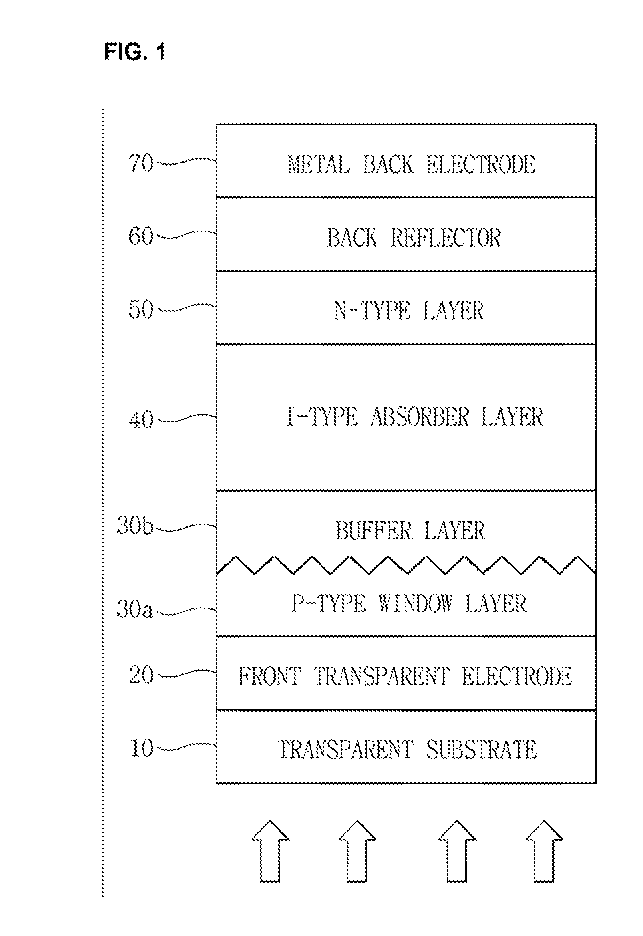
[0032]A thin film silicon solar cell according to the present embodiment has a structure in which a plurality of unit cells are electrically connected to each other in serial on a transparent substrate 10 such as a glass substrate or a transparent plastic substrate.

[0033]FIG. 1 is a cross-sectional view illustrating a single junction p-i-n type amorphous thin film silicon solar cell in accordance with an embodiment. Referring to FIG. 1, a thin film silicon solar cell includes a front transparent electrode 20 which is formed on a transparent substrate 10 and on which a surface texture is formed; an amorphous silicon carbide (p-a-SiC:H) window layer 30a (referred to as ‘p-type window layer’ hereinafter) low diluted with hydrogen on the front transparent electrode 20; an amorphous silicon carbide (p-a-SiC:H) buffer layer 30b (referred to as ‘buffer layer’ hereinafter) more highly diluted w...


PUM


Abstract

A thin film silicon solar cell comprises a front transparent electrode, a p-type window layer, a buffer layer, an i-type absorber layer, an n-type layer and a metal rear electrode. The front transparent electrode is stacked on a transparent substrate. The p-type window layer is stacked on the front transparent electrode, and has a thickness in a range of 12 nm to 17 nm. The buffer layer is stacked on the p-type window layer, and has a carbon concentration in a range of 0.5 to 3.0 atomic % and a thickness in a range of 3 to 8 nm. The i-type absorber layer is stacked on the buffer layer. The n-type layer is stacked on the i-type absorber layer. The metal rear electrode is stacked on the n-type layer.

Description

CROSS-REFERENCE TO RELATED APPLICATION[0001]This application is a divisional of U.S. patent application Ser. No. 12 / 421,184, filed Apr. 9, 2009 which claims priority to Korean Patent Application No. 10-2008-0033278 filed on Apr. 10, 2008, the entireties of which are hereby incorporated by reference.FIELD OF THE INVENTION[0002]The embodiment relates to a thin film silicon solar cell and manufacturing method thereof.BACKGROUND OF THE INVENTION[0003]Hydrogenated amorphous silicon (a-Si) solar cells have been widely studied due to high photosensitivity in a visible light region, easy control of an optical band gap, cost effective, low temperature, and large area process possibility. Further, there have been many attempts to reduce Stabler-Wronski effect of amorphous silicon materials. As a result, methods for diluting a silane (SiH4) with hydrogen (H2) have been developed.[0004]In order to develop high-efficiency thin film silicon solar cell, it is essential to form an absorber with a l...

Claims


Application Information

Patent Timeline
Patent Type & Authority Applications(United States)
IPC IPC(8): H01L31/0352H01L31/075
CPCH01L31/0745H01L31/075Y02E10/548H01L31/1812H01L31/076H01L31/18
Inventor MYONG, SEUNG-YEOP
Owner KISCO CORP (KR)
Why Eureka
Try Eureka