Solar cell having high quality back contact with screen-printed local back surface field

a solar cell and local back surface technology, applied in the field of solar cells with high quality back contact, can solve the problems of deformation of thin film silicon wafers, and inability to protect silicon wafers from the dielectric layer

Inactive Publication Date: 2009-01-29
GEORGIA TECH RES CORP
View PDF49 Cites 48 Cited by
  • Summary
  • Abstract
  • Description
  • Claims
  • Application Information

AI Technical Summary

Benefits of technology

[0011]The solution as presented herein comprises a solar cell structure that has a dielectric passivation layer and a rear contact with local aluminum back surface field. A process for forming the rear contact is provided. In an embodiment, a dielectric layer is formed on the rear surface of a thin crystalline wafer having an n-region and a p-region. An opening is made in the dielectric layer by screen printing an etch paste, followed by a first heat treatment. A hydrofluoric acid solution may be used to remove any residue left by the etch paste. The rear contact is formed by screen printing a contact paste on the entire back surface followed by a second heat treatment. The contact paste is comprised of aluminum and from one to 12 atomic percent silicon. The presence of the silicon in the contact paste saturates the appetite of aluminum for silicon during the second heat treatment, and provides a high-quality back surface field contact at the local openings. The use of little or no glass frit in the aluminum helps to avoid significant aluminum spiking through the dielectric layer which degrades device performance.

Problems solved by technology

This dielectric layer improves passivation, but creates other problems such as how to generate openings from the dielectric layer to the silicon, and optimizing the size and spacing of each window.
In addition, the dielectric layer does not protect the silicon wafer from aluminum-silicon alloying during contact formation, which may deform the silicon wafer.
Thin film silicon wafers are especially susceptible to deformation.
The prior art solutions for reducing recombination at the back surface do not adequately address other issues such as preventing thin film silicon deformation, determining the size and spacing of dielectric openings, cleaning the dielectric openings, and forming quality back surface fields at the dielectric openings.

Method used


Image

  • Solar cell having high quality back contact with screen-printed local back surface field
  • Solar cell having high quality back contact with screen-printed local back surface field
  • Solar cell having high quality back contact with screen-printed local back surface field

Examples


Embodiment Construction

[0024]In the following detailed description, numerous specific details are set forth in order to provide a thorough understanding of the invention. However, it will be understood by those skilled in the art that the present invention may be practiced without these specific details. In other instances, well-known methods, procedures, components, and circuits have not been described in detail so as not to obscure the present invention.

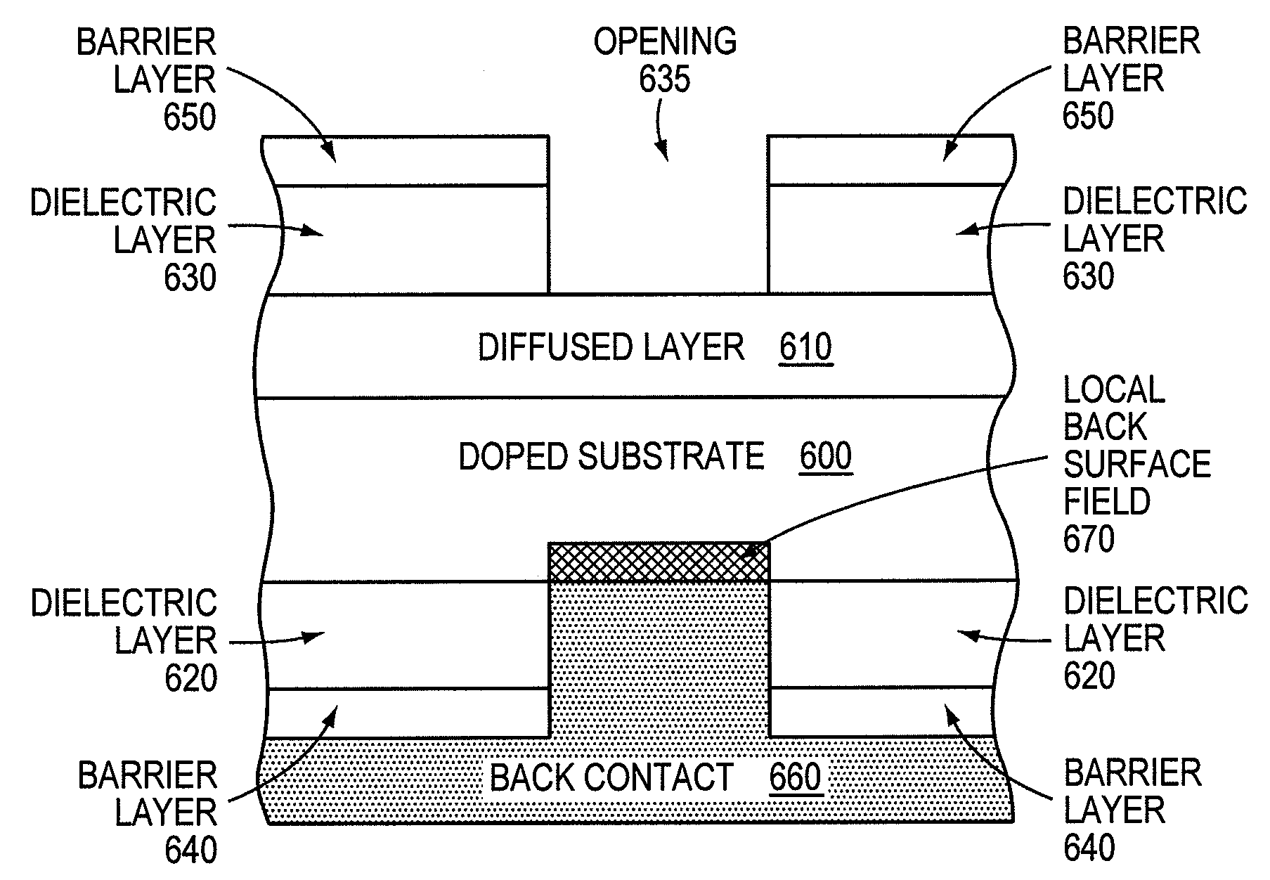
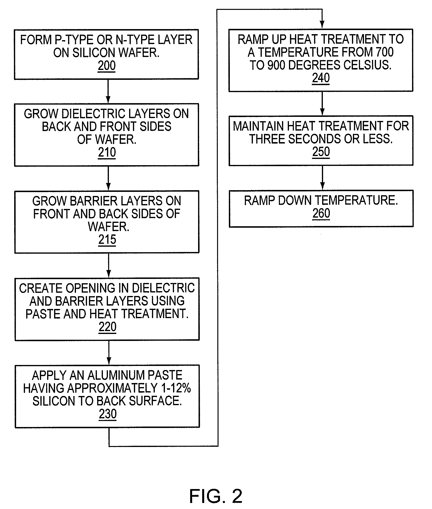
[0025]FIG. 2 depicts a flowchart for forming a high quality rear contact that protects the silicon wafer from damage during the alloying process and provides a local back surface field. A local back surface field (BSF) is desirable because it helps to reduce the recombination of electrons at the solar cell's back surface. Efficiency of the solar cell is thereby increased if the solar cell has a high quality local BSF.

[0026]In operation 200, a p-type or n-type layer is formed on a silicon wafer. The silicon wafer may be crystalline. The silicon wafer may ...


PUM


Abstract

A thin silicon solar cell having a back dielectric passivation and rear contact with local back surface field is described. Specifically, the solar cell may be fabricated from a crystalline silicon wafer having a thickness from 50 to 500 micrometers. A barrier layer and a dielectric layer are applied at least to the back surface of the silicon wafer to protect the silicon wafer from deformation when the rear contact is formed. At least one opening is made to the dielectric layer. An aluminum contact that provides a back surface field is formed in the opening and on the dielectric layer. The aluminum contact may be applied by screen printing an aluminum paste having from one to 12 atomic percent silicon and then applying a heat treatment at 750 degrees Celsius.

Description

CROSS REFERENCE TO RELATED APPLICATIONS[0001]The present application claims priority to and the benefit of U.S. Provisional Patent Application No. 60 / 916,327, filed May 7, 2007.GOVERNMENT INTERESTS[0002]The U.S. Government has a paid-up nonexclusive, worldwide license in this invention and the right in limited circumstances to require the patent owner to license others on reasonable terms as provided for by the terms of contract No. DE-FC36-07GO17023 awarded by the U.S. Department of Energy.FIELD OF THE INVENTION[0003]The present invention generally relates to silicon solar cells. More particularly, the present invention relates to a formation of a back or rear contact that provides back surface passivation and optical confinement properties.BACKGROUND OF THE INVENTION[0004]Solar cells are devices that convert light energy into electrical energy. These devices are also often called photovoltaic (PV) cells. Solar cells are manufactured from a wide variety of semiconductors. One commo...

Claims


Application Information

Patent Timeline
Patent Type & Authority Applications(United States)
IPC IPC(8): H01L31/00
CPCH01L31/022425H01L31/068Y02E10/547H01L31/1868H01L31/1804Y02P70/50
Inventor ROHATGI, AJEETMEEMONGKOLKIAT, VICHAI
Owner GEORGIA TECH RES CORP
Why Eureka
Try Eureka