

Making method for selective transmission node crystal silicon solar battery
A technology of silicon solar cells and crystals, applied in circuits, electrical components, semiconductor devices, etc., can solve the problems of high price, high cost, and low requirements for graphic precision, achieve low equipment investment, high production efficiency, and overcome equipment investment expensive effect
- Summary
- Abstract
- Description
- Claims
- Application Information
AI Technical Summary
Problems solved by technology
Method used
Image

Examples
Embodiment 1
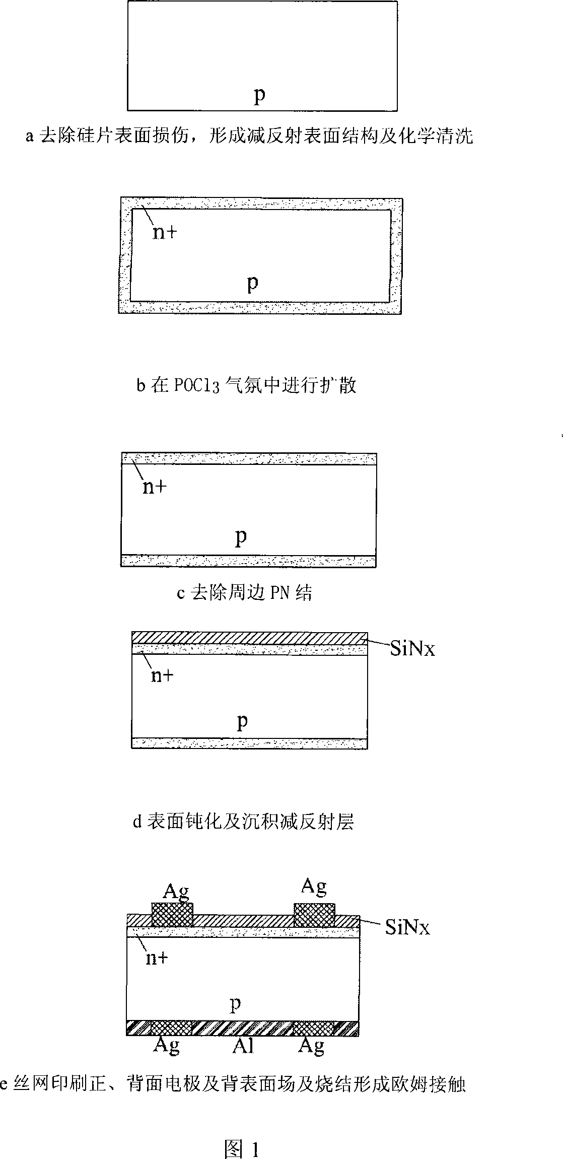
[0035] Embodiment 1: As shown in FIG. 3 , a method for preparing a selective emission crystalline silicon solar cell. First high-concentration diffusion, then low-concentration diffusion embodiment, the process is as follows:
[0036] 1. Remove the surface damage of the silicon wafer, form an anti-reflection surface structure and chemical cleaning.
[0037] 2. Thermal oxidation growth of silicon dioxide layer.
[0038] 3. On the silicon dioxide layer of the crystalline silicon wafer, the etchant is printed by printing process, and the electrode window is formed by etching, and then, in the electrode window area, POCl 3 Diffusion of high-concentration doping is carried out in the atmosphere. The process steps of printing etchant and corroding to form the electrode window are:
[0039] The etchant is printed on the surface of the silicon wafer with a silicon dioxide layer where electrodes need to be made (the printing process is the same as that of printing the front and back...
Embodiment 2
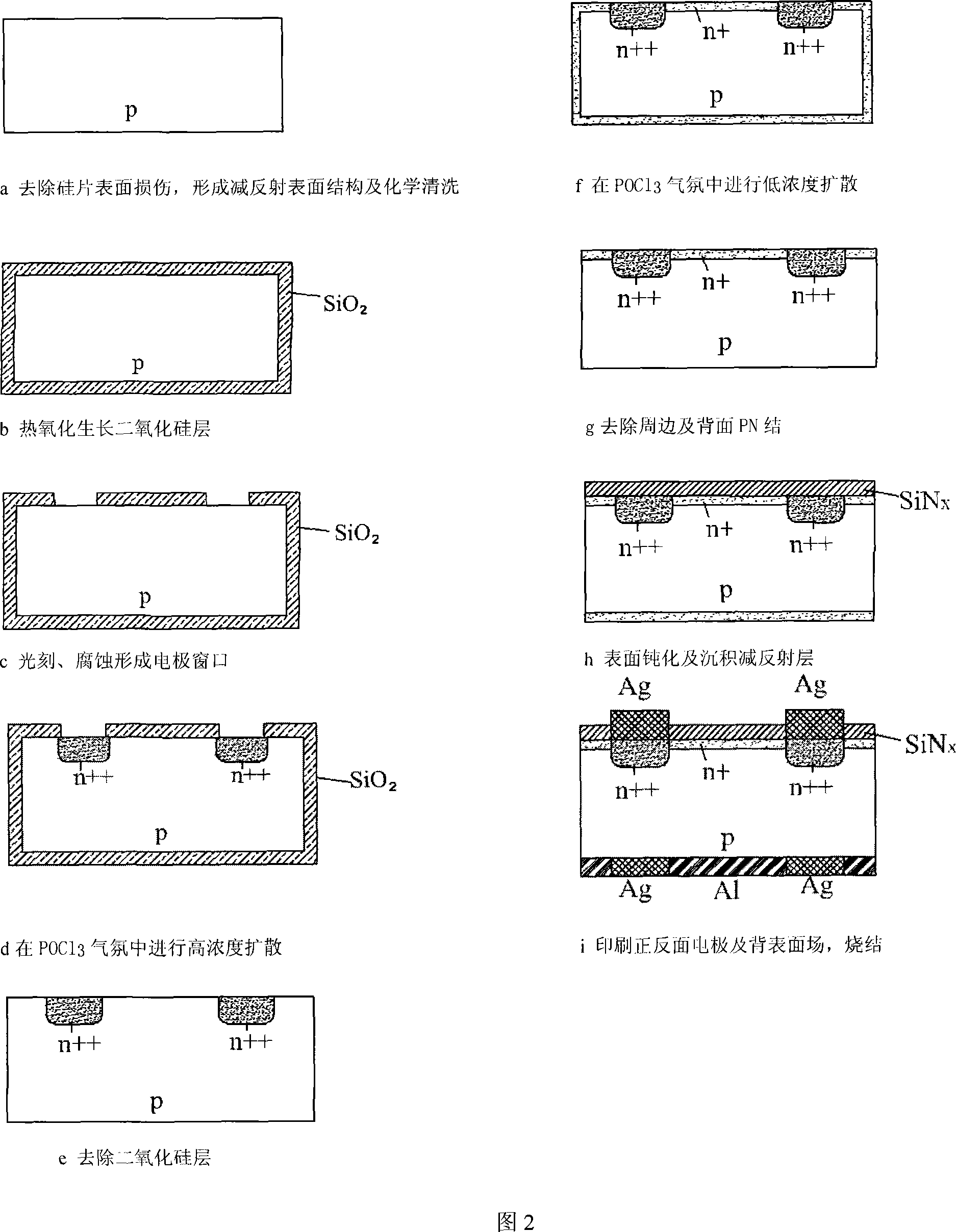
[0046] Embodiment 2, as shown in FIG. 4 , a method for preparing a selective emission crystalline silicon solar cell. Low-concentration diffusion first, followed by high-concentration diffusion embodiment, the process is as follows:
[0047] Remove surface damage of silicon wafer, form anti-reflection surface structure and chemical cleaning. crystalline silicon wafer in POCl 3Carry out low-concentration diffusion in the atmosphere, then thermally oxidize and grow a silicon dioxide layer on the surface of the diffused crystalline silicon wafer, and then print an etchant on the silicon dioxide layer where electrodes need to be made, and the etchant is ammonium bifluoride with a concentration of 25% . After the etchant fully corrodes the silicon dioxide layer on the surface of the silicon wafer to be used as an electrode, the silicon wafer is cleaned to remove the etchant and form an electrode window. In the electrode window area the POCl 3 Diffusion of high-concentration dop...
Embodiment 3
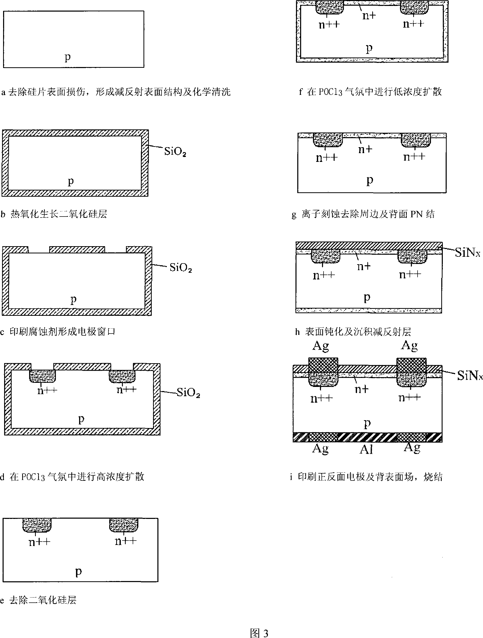
[0048] Embodiment 3, as shown in FIG. 5 , a method for preparing a selective emission crystalline silicon solar cell. The embodiment of simultaneous high and low concentration diffusion, the process steps are as follows:
[0049] Remove surface damage of silicon wafer, form anti-reflection surface structure and chemical cleaning. Thermally oxidize and grow a silicon dioxide layer on the surface of the crystalline silicon wafer, the thickness of the silicon dioxide layer is 6nm; use a printing process to print an etchant on the silicon dioxide layer of the crystalline silicon wafer, and the etchant is ammonium bifluoride with a concentration of 20%, etch to form electrode windows, and then, the POCl 3 Doping diffusion is carried out in the atmosphere, forming high-concentration doping diffusion in the electrode window area, and forming high-concentration doping diffusion in other areas of the crystalline silicon wafer. Remove the peripheral and back PN junctions. Surface pas...
PUM
 Abstract
Description
Claims
Application Information