Aluminum pastes and use thereof in the production of silicon solar cells

a technology of silicon solar cells and aluminum pastes, applied in the field of aluminum pastes, can solve the problems of reducing the solderability and adhesion of ribbons tabbed to said surface, and achieve the effect of reducing the solderability and adhesion

Inactive Publication Date: 2009-09-17
EI DU PONT DE NEMOURS & CO
View PDF5 Cites 48 Cited by
  • Summary
  • Abstract
  • Description
  • Claims
  • Application Information

AI Technical Summary

Benefits of technology

[0017]The present invention is further directed to a process of forming a silicon solar cell and the silicon solar cell itself which utilizes a silicon wafer having a p-type and an n-type region, and a p-n junction, which comprises applying, in particular, screen-printing an aluminum paste of the present invention on the back-side of the silicon wafer, and firing the printed surface, whereby the wafer reaches a peak temperature in the range of 700 to 900° C.

Problems solved by technology

A problem associated with the aluminum paste is dusting and transfer of free aluminum or alumina dust to other metallic surfaces, thereby reducing the solderability and adhesion of ribbons tabbed to said surface.

Method used


Image

  • Aluminum pastes and use thereof in the production of silicon solar cells
  • Aluminum pastes and use thereof in the production of silicon solar cells
  • Aluminum pastes and use thereof in the production of silicon solar cells

Examples


examples

[0077]The examples cited here relate to thick-film metallization pastes fired onto conventional solar cells that have a silicon nitride anti-reflection coating and front side n-type contact thick film silver conductor.

[0078]The present invention can be applied to a broad range of semiconductor devices, although it is especially effective in light-receiving elements such as photodiodes and solar cells. The discussion below describes how a solar cell is formed utilizing the composition(s) of the present invention and how it is tested for its technological properties.

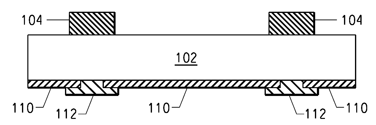
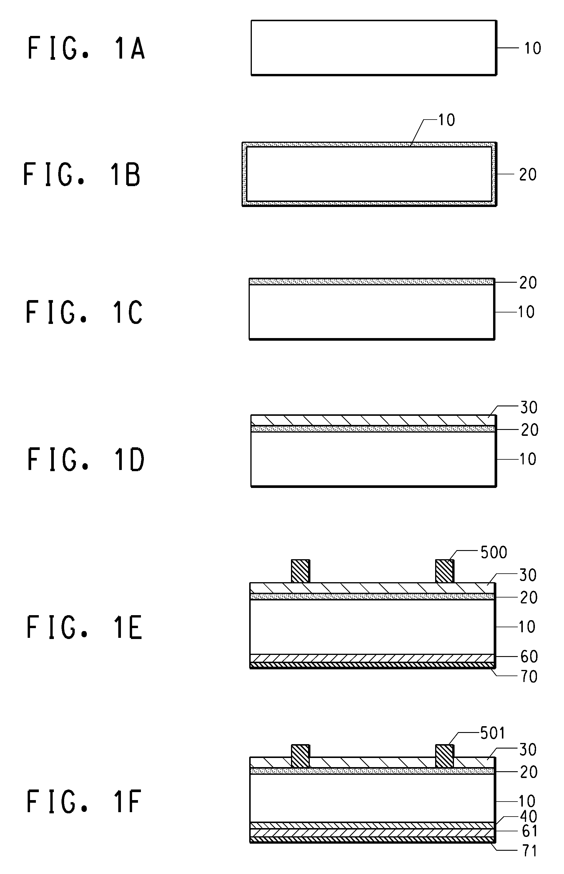
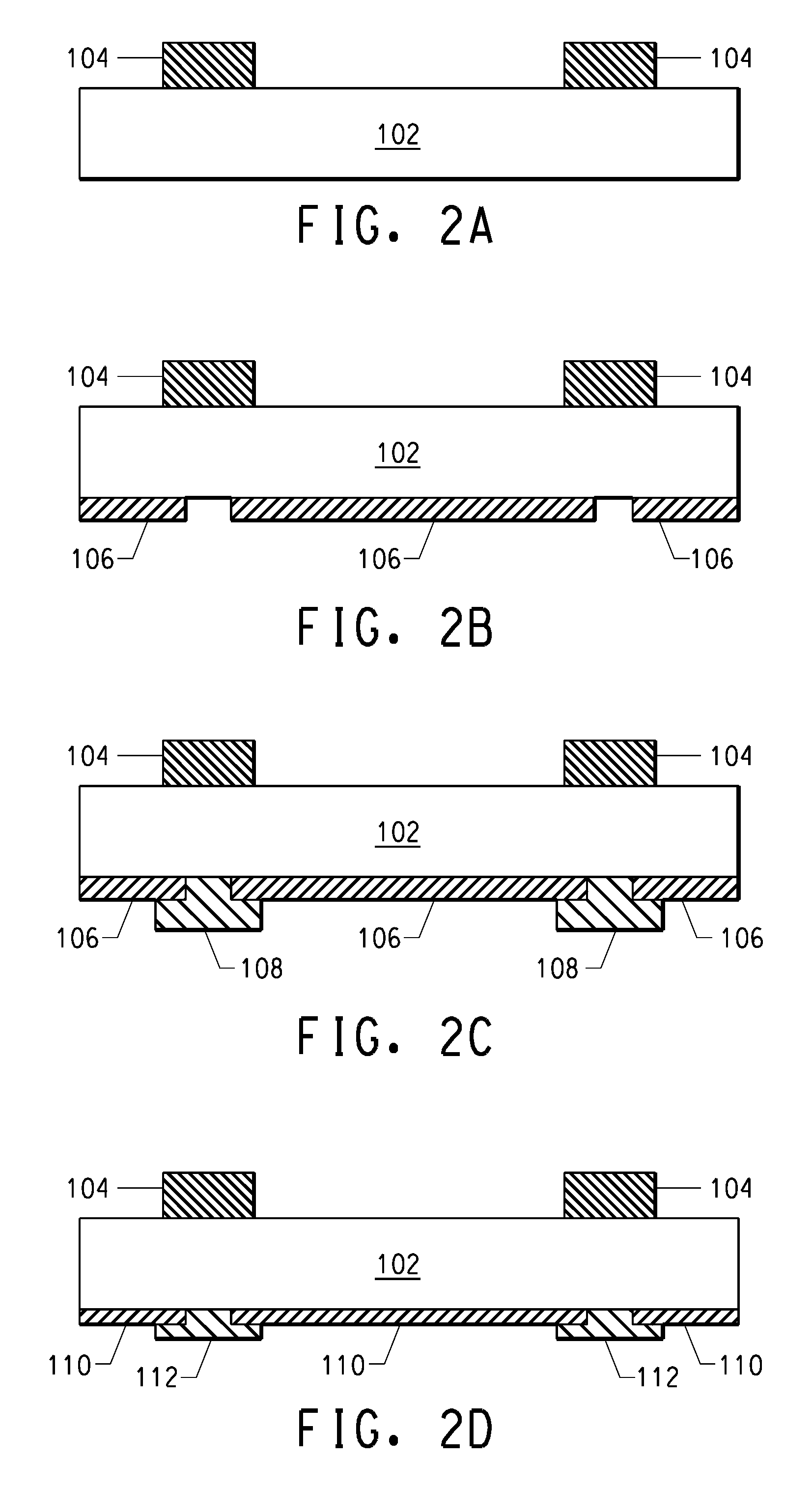
(1) Manufacture of Solar Cell

[0079]A solar cell was formed as follows:

[0080](i) On the back face of a Si substrate (200 μm thick multicrystalline silicon wafer of area 243 cm2, p-type (boron) bulk silicon, with an n-type diffused POCl3 emitter, surface texturized with acid, SiNx anti-reflective coating (ARC) on the wafer's emitter applied by CVD) having a 20 μm thick silver electrode on the front surface (PV145 Ag composit...


PUM

PropertyMeasurementUnit
wt. %aaaaaaaaaa
temperatureaaaaaaaaaa
junction depthaaaaaaaaaa

Abstract

Disclosed are aluminum pastes comprising particulate aluminum, a zinc-organic component and an organic vehicle and their use in forming p-type aluminum back electrodes of silicon solar cells.

Description

FIELD OF THE INVENTION[0001]The present invention is directed to aluminum pastes, and their use in the production of silicon solar cells, i.e., in the production of aluminum back electrodes of silicon solar cells and the respective silicon solar cells.TECHNICAL BACKGROUND OF THE INVENTION[0002]A conventional solar cell structure with a p-type base has a negative electrode that is typically on the front-side or sun side of the cell and a positive electrode on the back-side. It is well known that radiation of an appropriate wavelength falling on a p-n junction of a semiconductor body serves as a source of external energy to generate hole-electron pairs in that body. The potential difference that exists at a p-n junction, causes holes and electrons to move across the junction in opposite directions and thereby give rise to flow of an electric current that is capable of delivering power to an external circuit. Most solar cells are in the form of a silicon wafer that has been metalized, ...

Claims


Application Information

Patent Timeline
Patent Type & Authority Applications(United States)
IPC IPC(8): H01L31/00H01L21/00H01L31/18
CPCH01B1/22Y02E10/50H01L31/022425
Inventor YOUNG, RICHARDROSE, MICHAELPRINCE, ALISTAIR GRAEME
Owner EI DU PONT DE NEMOURS & CO
Why Eureka
Try Eureka