

Laser structuring for manufacture of thin film silicon solar cells
a technology of solar cells and lasers, applied in the field of solar cells, can solve the problems of high module fill factor, inconvenient scribing of zno tco layer, and inability to use 1064 nm lasers for functioning,
Inactive Publication Date: 2005-12-08
OERLIKON TRADING AG TRUEBBACH
View PDF9 Cites 48 Cited by
- Summary
- Abstract
- Description
- Claims
- Application Information
AI Technical Summary
Benefits of technology
[0018] providing an additional conducting layer on the one or more active layers.
Problems solved by technology
Furthermore, in the case of LP-CVD (low pressure chemical vapor deposition) ZnO fabrication of the TCO layer, use of the 1064 nm lasers for the realization of functioning, large-area a-Si:H (amorphous hydrogenated silicon) anhydrous-based PV modules has not been commercially successful.
Thus, use of 532 nm lasers did not lead to a high fill factor of the module, as desired, and thus were not useful for scribing a ZnO TCO layer.
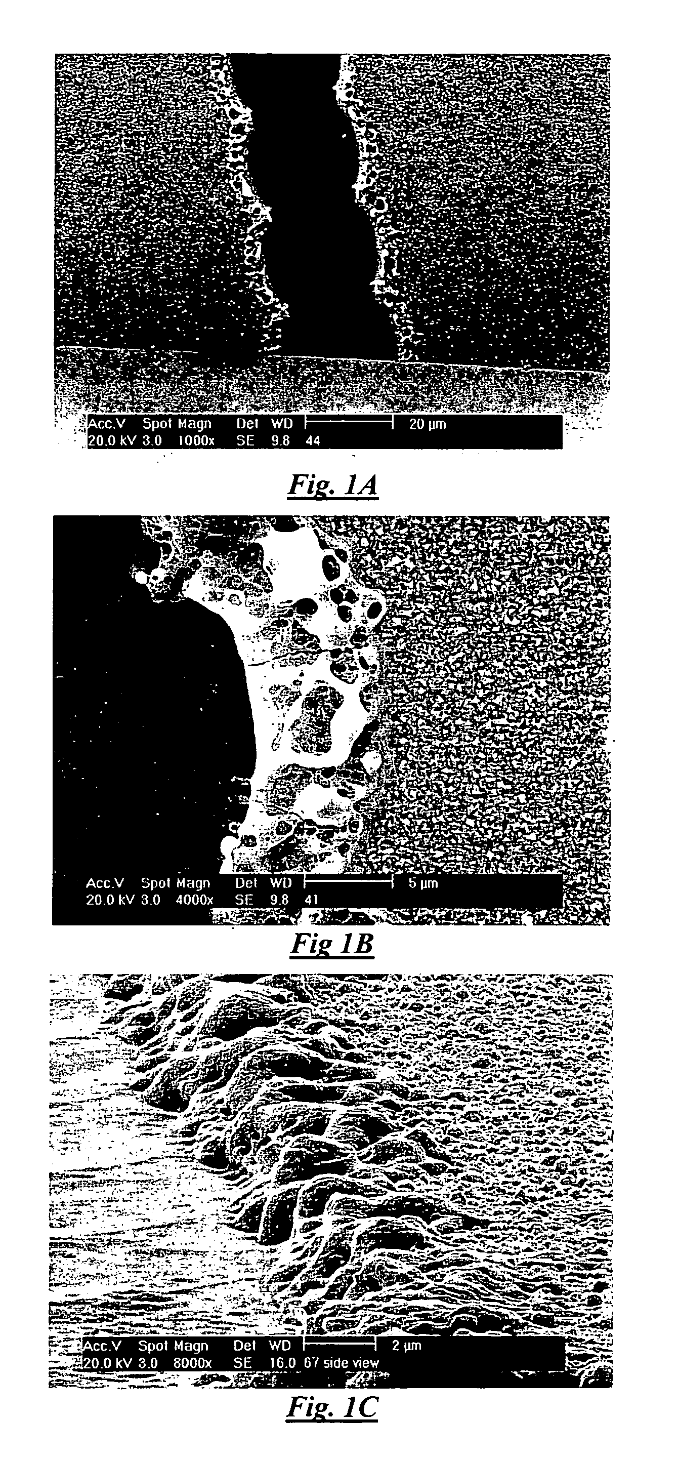
However, FIGS. 1A, 1B, and 1C highlight two problems resulting from the structuring of the ZnO TCO scribes using the 1064 nm scribing laser: (1) the difficulty of realizing an electrical isolation of the TCO segments of at least several 100 kΩ / meter and (2) the lack of quality of the edges of the resulting trench cuts.
These short-circuits can then lead to a dramatic and undesirable loss in the efficiency of the modules.
Thus, the use of 1064 nm laser scribing cannot be effectively applied even when a good isolation is achieved.
Because the structuring of ZnO using lasers at 1064 nm wavelength result in undesirable burn-outs, the use of ZnO for the TCO layer has been unsatisfactory, because the borders of the trench cuts through ZnO using the 1064 nm laser resulted in the irregular bulges or beads with a sharp texture, as discussed above, compared to as-grown textured LP-CVD ZnO.
A further disadvantage of the use of the 1064 nm laser scribing process was the low process speed of the cutting (scribing) velocities, which were typically below 10 m / min.
An additional disadvantage was the wide trench width, which is typically larger than 20 μm, leading to wasted space.
These disadvantages make the overall module less efficient than it could be.
Method used
View moreImage
Smart ImageViewing Examples

Examples
example application
[0056] Specifications of an applied UV-laser (Coherent AVIA 355-X used successfully according to the invention are:
Wavelength:355 nmPower:10.0 Watt at 60 kHzPulse frequency range:1 Hz to 100 kHzPulse length:M2:Polarization:>100:1, horizontalBeam diameter (exit):3.5 mm at 1 / e2Beam divergence at full angle:
[0057] ZnO layers for the sample were about 2 μm thick deposited on glass by LP-CVD process.
[0058] Laserscribing or layer structuring processes for coated substrates with ZnO deposited by other methods (sputtering, etc.) or other TCO materials with similar absorption characteristics to ZnO could also benefit from the described process of the invention as well.
Login to View More PUM
| Property | Measurement | Unit |
|---|---|---|
| wavelength | aaaaa | aaaaa |
| wavelength | aaaaa | aaaaa |
| width | aaaaa | aaaaa |
Abstract
A method of manufacturing thin-film, series connected silicon solar cells having a ZnO TCO layer, for example, using an ultraviolet scribing laser to scribe said ZnO TCO layer to form relatively smooth walls through said TCO layer.
Description
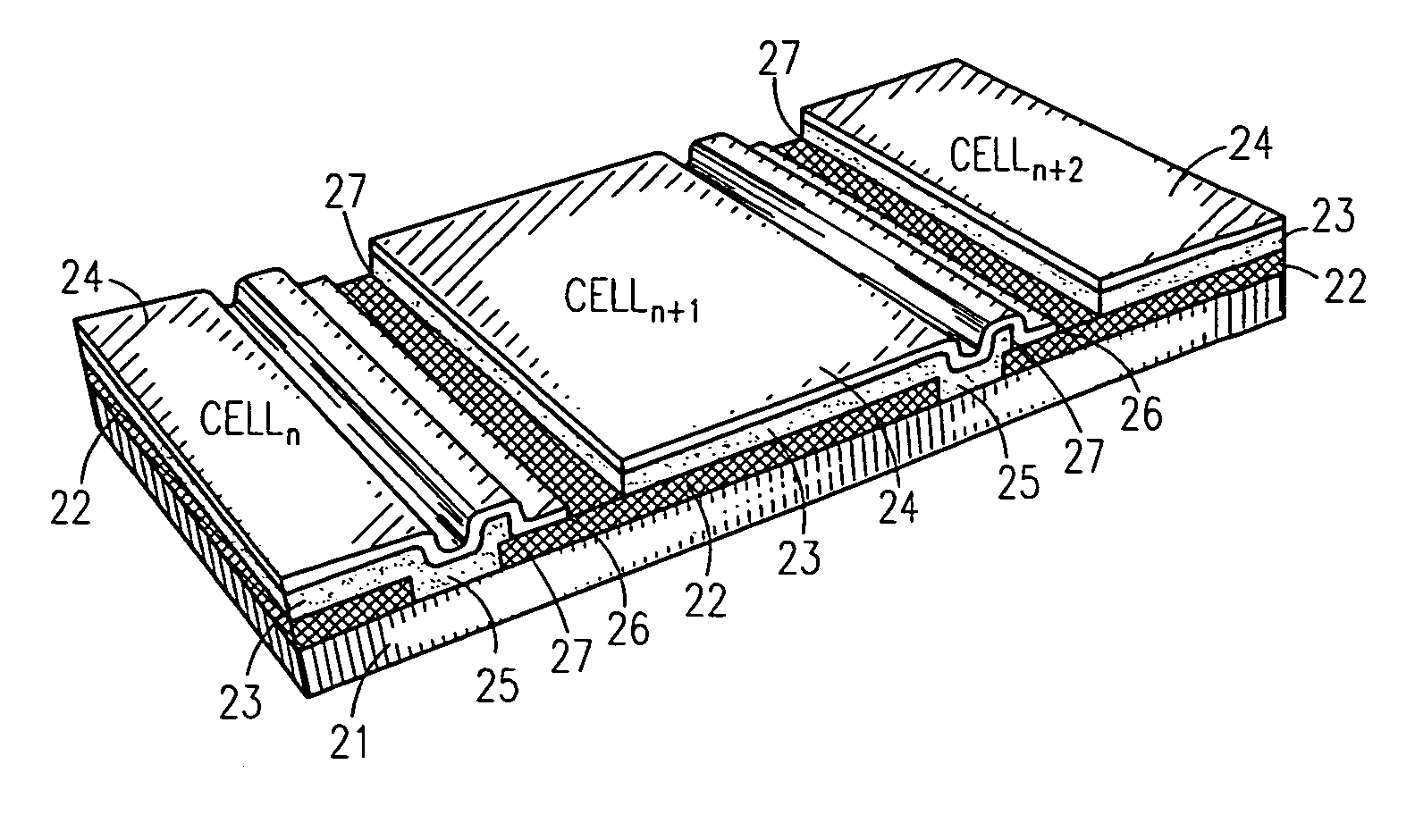
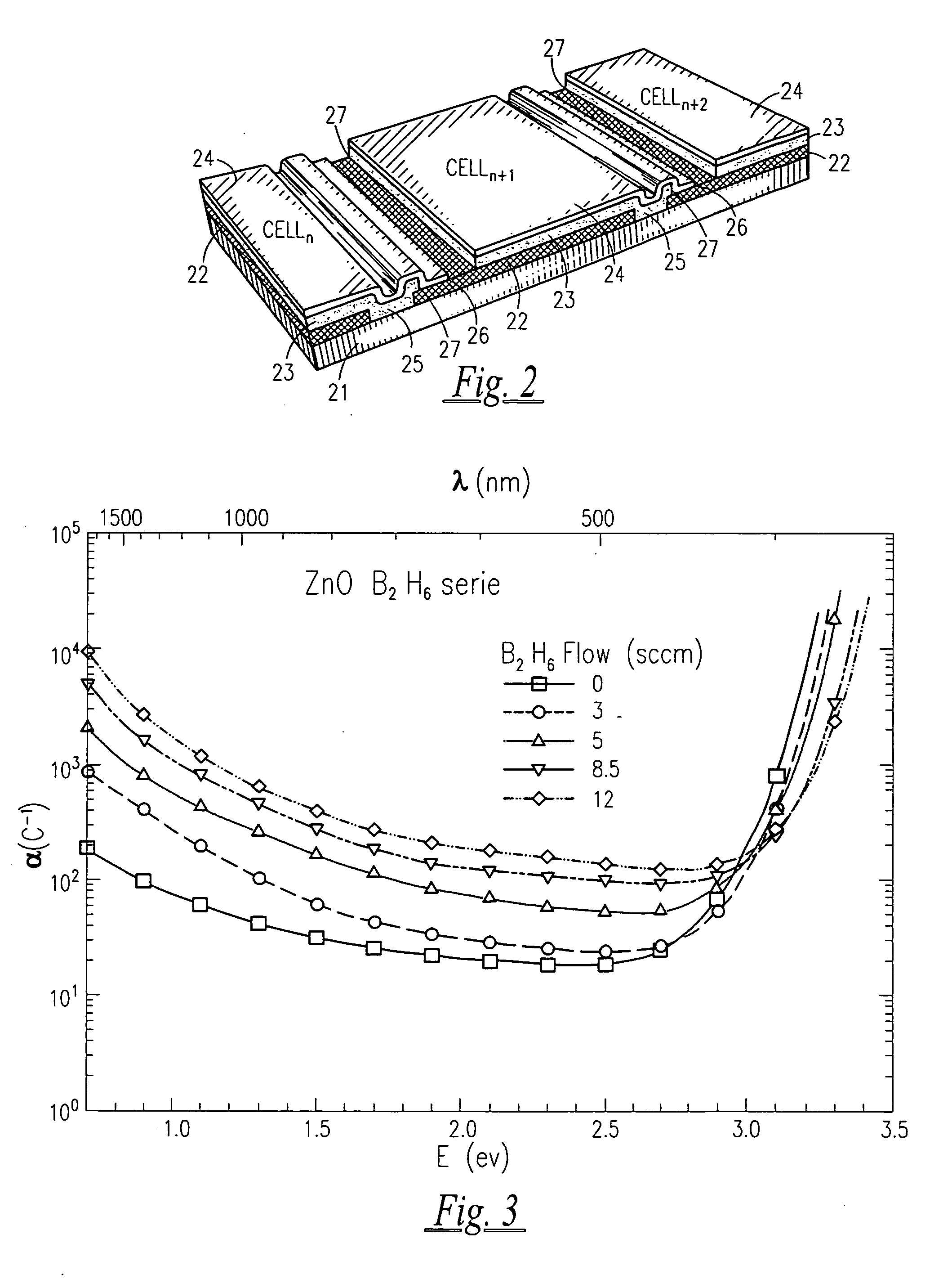
CROSS-REFERENCES TO RELATED APPLICATIONS [0001] This application claims the benefit of provisional application Ser. No. 60 / 576,142, filed on Jun. 2, 2004, incorporated herein by reference.BACKGROUND OF THE INVENTION [0002] This application relates generally to a solar cell and its method of manufacture. More specifically, this application relates to a method of manufacturing thin-film, series connected silicon solar cells using an ultraviolet scribing laser. [0003] Thin film solar cells having monolithic series interconnections can be formed by using laser or mechanical structuring. Mechanical structuring can include photolithographic or chemical etching structuring. The structuring is useful to form large-area photovoltaic (PV) modules or “arrays”. These concepts allow the PV modules to be adapted to the desired output characteristics—VOC (open circuit voltage), ISC (short-circuit-current) and FF (fill factor—defined as the maximum power produced at the maximum power point, divided...
Claims
Login to View More Application Information
Patent Timeline
 Patent Type & AuthorityApplications(United States)
IPC IPC(8): B23K26/40H01L21/00H01L27/142H01L31/0224H01L31/18
CPCH01L31/1884Y02E10/50H01L31/046B23K26/364B23K2103/50H01L31/0463H01L31/022483B23K2103/172B23K26/40
InventorMEIER, JOHANNESGRUNDMULLER, RICHARD
OwnerOERLIKON TRADING AG TRUEBBACH