Fabrication method of double-side PERC crystalline silicon solar cell

A technology of solar cells and crystalline silicon, applied in semiconductor/solid-state device manufacturing, circuits, photovoltaic power generation, etc., to achieve the effect of improving conversion efficiency

Inactive Publication Date: 2018-03-30
SPIC XIAN SOLAR POWER CO LTD
View PDF11 Cites 52 Cited by
  • Summary
  • Abstract
  • Description
  • Claims
  • Application Information

AI Technical Summary

Problems solved by technology

[0004] However, the conversion efficiency of bifacial PERC solar cells still needs to be further improved

Method used


Image

  • Fabrication method of double-side PERC crystalline silicon solar cell
  • Fabrication method of double-side PERC crystalline silicon solar cell

Examples


preparation example Construction

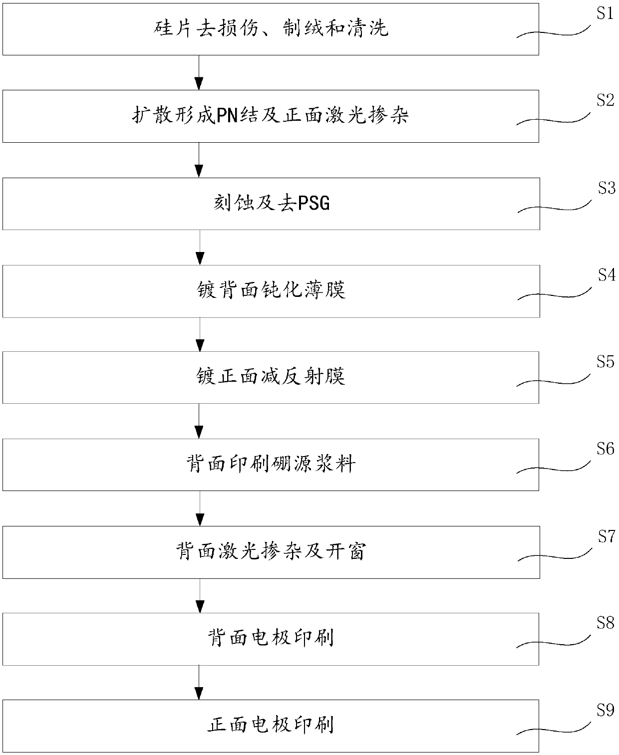
[0032] Such as figure 2 As shown, the preparation method of the double-sided PERC crystalline silicon solar cell provided by the embodiment of the present invention includes the following steps:

[0033] S1: Silicon wafer damage removal, texturing and cleaning: After removing the damaged layer of the silicon wafer, texture it in a lye and additive system at a temperature of 80-85°C to form a textured surface on the front and back of the silicon wafer, and then Cleaning in solution to remove surface impurities;

[0034] S2: Diffusion to form a PN junction and front-side laser doping: Perform high-temperature phosphorus diffusion on silicon wafers to form a PN junction. The diffusion temperature is 830-860°C, the diffusion time is 80-100 minutes, and the surface sheet resistance after diffusion is 130-160Ω / □ , use the laser to heat the front side of the silicon wafer, push the phosphorus atoms in the phosphosilicate glass into the PN junction, form the corresponding N++ layer,...

Embodiment 1

[0045] The manufacturing method of the double-sided PERC crystalline silicon solar cell provided in this embodiment includes the following steps:

[0046](1) Texturing: Select a P-type diamond wire-cut monocrystalline silicon wafer with a size of 156.75 mm×156.75 mm and a resistivity of 2.5 Ω cm as the base material, and put it into hydrogen oxide with a mass percentage concentration of 3% heated to 80°C. In a mixed solution of sodium and additives with a mass percentage concentration of 1.5%, the corrosion reaction takes 20 minutes, the thinning of the texture is 0.60g, and the size of the bottom of the pyramid of the texture is about 2.0mm. The additive is a conventional texture additive, and its main component is water. , IPA (isopropanol), NaOH, weak acid salt; after texturing, use HF / HCl mixed acid solution to clean the silicon wafers after texturing at room temperature, the volume percentage concentration of HF is 5%, and the volume percentage concentration of HCl is 5%. ...

Embodiment 2

[0058] The manufacturing method of the double-sided PERC crystalline silicon solar cell provided in this embodiment includes the following steps:

[0059] (1) Texturing: select 156.75mm * 156.75mm, the P-type diamond wire-cut monocrystalline silicon slice of resistivity 2Ω cm as the base material, put into the mass percentage concentration that is heated to 80 ℃ and be 3% sodium hydroxide, In an additive mixed solution with a mass percentage concentration of 1.5%, the corrosion reaction takes 18 minutes, the thinning of the textured surface is 0.55 g, and the bottom size of the pyramid of the textured surface is about 1.8 mm; after the textured surface, the mixed acid solution of HF / HCl is used to clean the textured textured surface at room temperature. For silicon wafers, the concentration of HF volume percentage is 4%, the volume percentage concentration of HCl is 4%, and the surface reflectance of silicon wafers after texturing is 10.5%;

[0060] (2) Diffusion: The method o...


PUM

PropertyMeasurementUnit
electrical resistivityaaaaaaaaaa
widthaaaaaaaaaa
thicknessaaaaaaaaaa

Abstract

The invention discloses a fabrication method of a double-side PERC crystalline silicon solar cell. The fabrication method comprises the following steps of (1) removing damage of a silicon wafer, and performing texturing and cleaning; (2) performing diffusion to form a pn junction and performing front-surface laser doping; (3) etching and removing PSG; (4) plating a back-surface passivation thin film; (5) plating a front-surface anti-reflection film; (6) printing boron source paste on a back surface; (7) performing back-surface laser doping and windowing; (8) performing back-surface electrode printing; and (9) performing front-surface electrode printing. A laser doping technology is applied to a process of a selective emitter formed on a front surface and local boron doping on the back surface, only two processes of laser doping and boron source paste printing are added on the basis of a conventional PERC battery process, and the conversion efficiency of the double-side PERC cell is greatly improved; moreover, with the adoption of a secondary printing alignment laser printing MARK point mode, the back-surface metallization of the double-side PERC cell is achieved; and by the method,the problem of difficulty in alignment of a back-surface aluminum grid line to a laser windowing grid line of the silk-screen printed double-sided PERC cell is completely solved.

Description

technical field [0001] The invention relates to the technical field of manufacturing crystalline silicon solar cells, in particular to a method for preparing double-sided PERC crystalline silicon solar cells. Background technique [0002] Achieving "grid parity" is the key to the sustainable development of the photovoltaic industry. Reducing the cost of photovoltaics requires not only economies of scale, but also technological innovation and application. Passivated Emitter and Rear Surface (PERC) technology is the most cost-effective means of improving the efficiency of crystalline silicon solar cells in recent years. Conversion efficiency of polycrystalline cells. The market's pursuit of high-efficiency components has further enhanced the competitiveness of PERC cells. [0003] The directions for further improving the efficiency of P-type PERC cells include selective emitter on the front side and local boron doping on the back side. In addition, PERC is the simplest and ...

Claims


Application Information

Patent Timeline
Patent Type & Authority Applications(China)
IPC IPC(8): H01L31/18H01L31/0224H01L21/22H01L21/223H01L21/268
CPCH01L21/2225H01L21/223H01L21/268H01L31/022425H01L31/18Y02E10/50Y02P70/50
Inventor 吴翔
Owner SPIC XIAN SOLAR POWER CO LTD
Why Eureka
Try Eureka