Embedded printed circuit board, multi-layer printed circuit board and manufacturing method thereof

Active Publication Date: 2011-06-02
LG INNOTEK CO LTD
View PDF4 Cites 13 Cited by
  • Summary
  • Abstract
  • Description
  • Claims
  • Application Information

AI Technical Summary

Benefits of technology

[0030]According to the present invention, the method of manufacturing an embedded PCB can simultaneously or sequentially etch a photoresist layer and an insulating layer using a laser to form a circuit pattern

Problems solved by technology

However, the above conventional processes are difficult to secure reliability in micro circuits because of a variation in patterns during photolithography and adhesion of materials in the micro circuits.
However, the above conventional method of manufacturi

Method used


Image

  • Embedded printed circuit board, multi-layer printed circuit board and manufacturing method thereof
  • Embedded printed circuit board, multi-layer printed circuit board and manufacturing method thereof
  • Embedded printed circuit board, multi-layer printed circuit board and manufacturing method thereof

Examples


Example

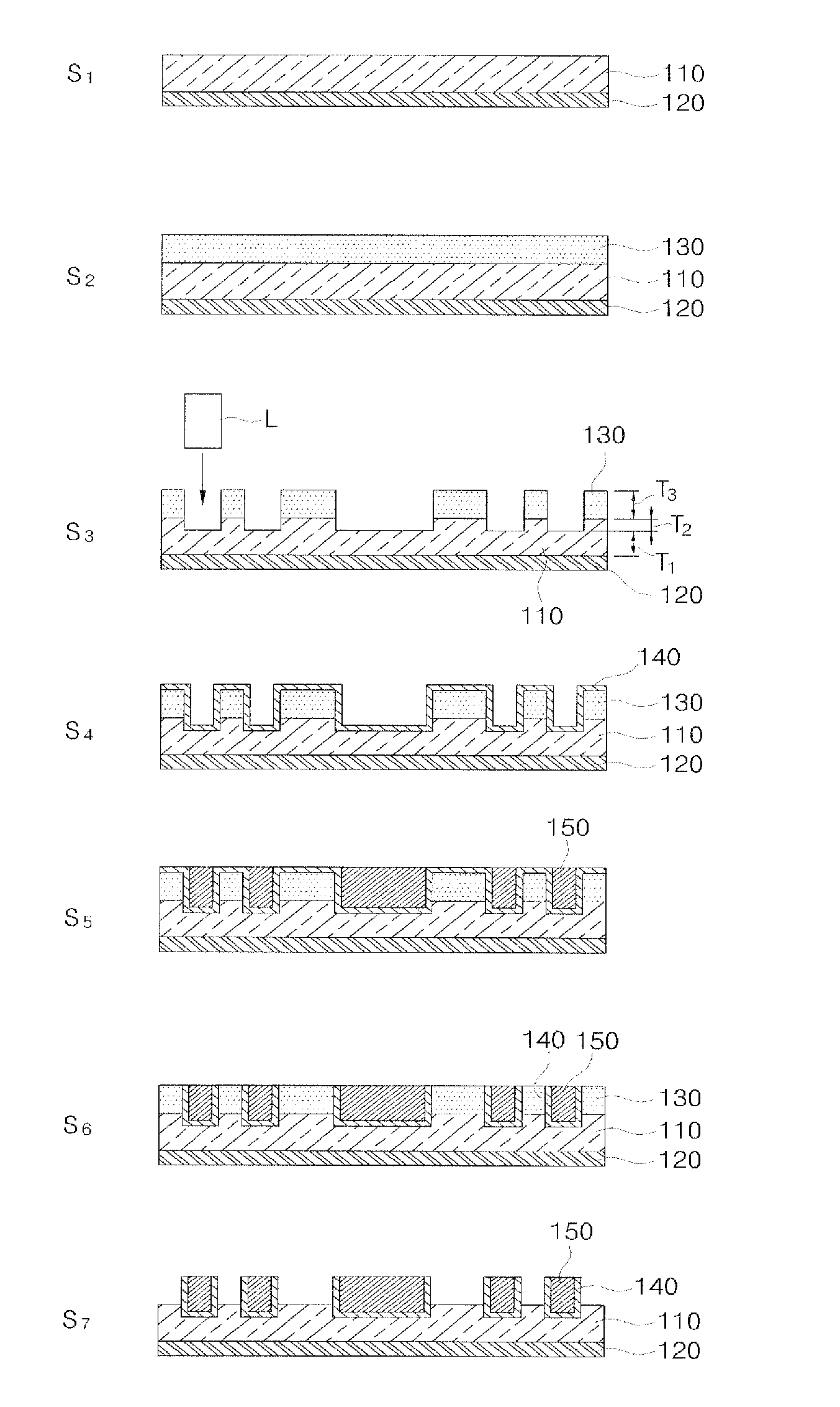
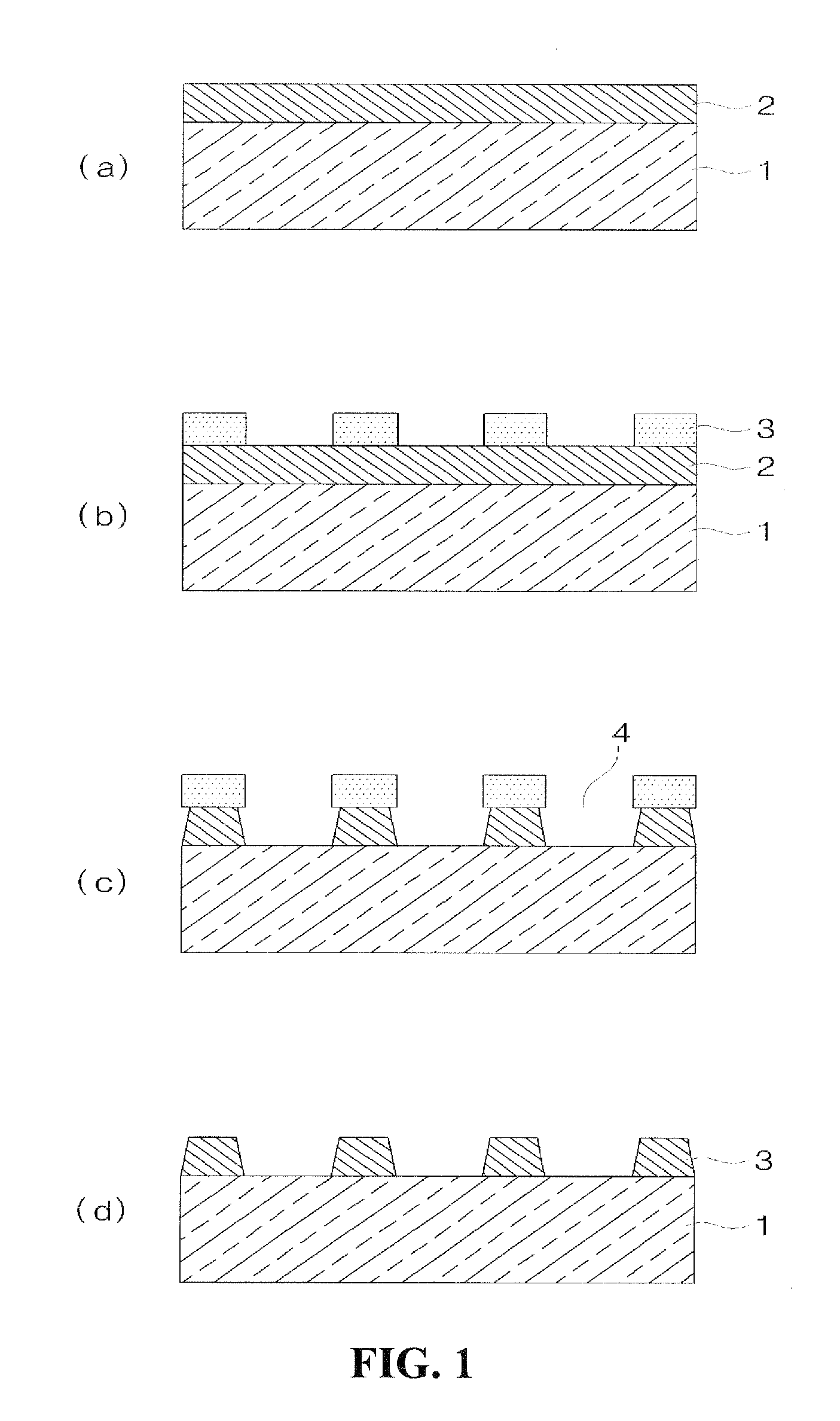
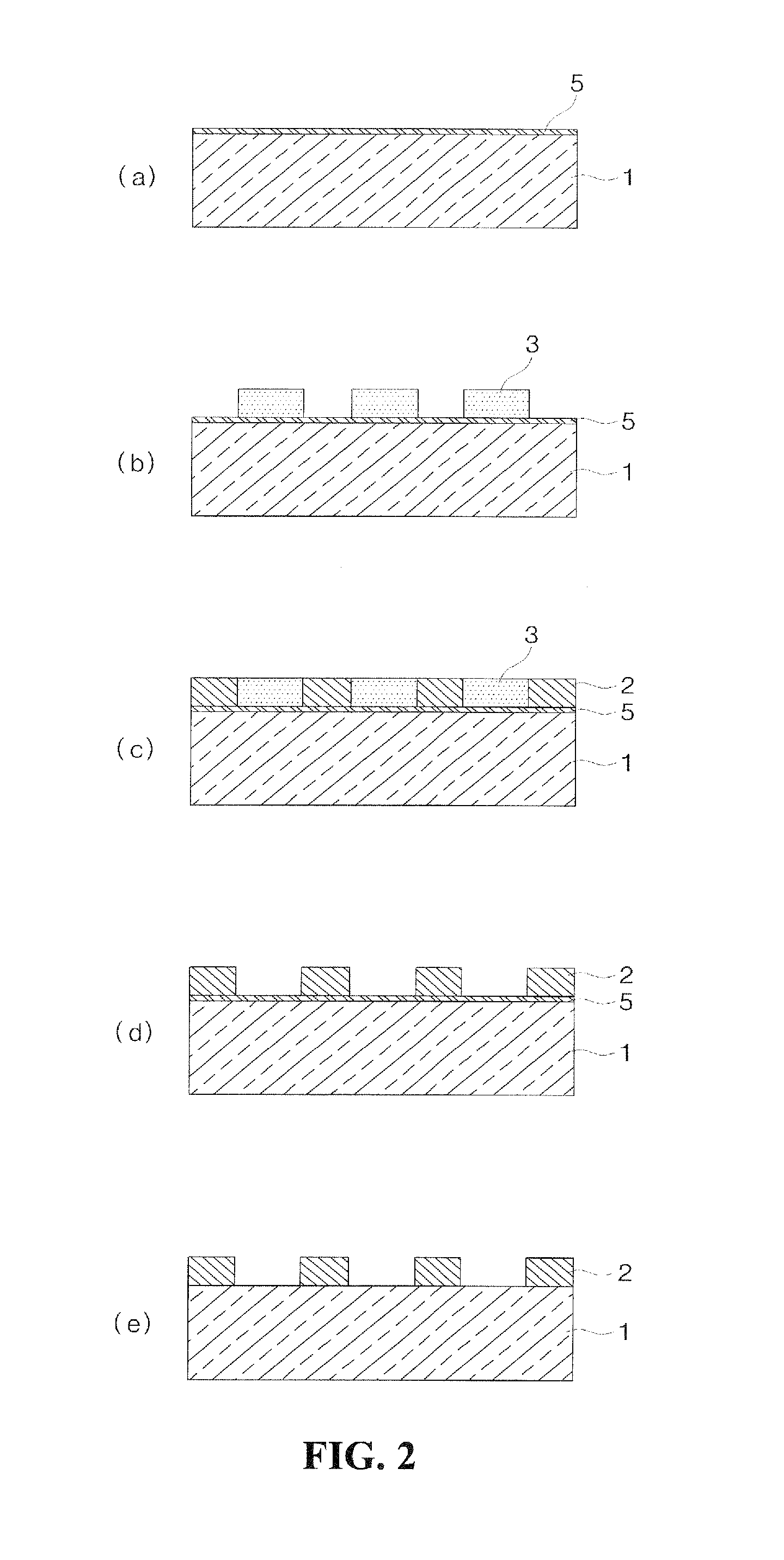
[0036]In methods of manufacturing an embedded PCB and a multi-layer PCB using the embedded PCB, the present invention processes photoresist and an insulating layer using a laser to form a circuit pattern so as to simplify a manufacturing process and improve the reliability of accomplished products.

[0037]A method of manufacturing an embedded PCB according to the present invention comprises a first step of patterning an insulating layer on which a photoresist layer is formed using a laser such that parts of the insulating layer are selectively etched to form a circuit pattern region and a second step of filling the circuit pattern region with a plating material to form a circuit pattern. The manufacturing method may further comprise a step of removing the photoresist layer.

[0038]The present invention will now be described more fully with reference to the accompanying drawings, in which exemplary embodiments of the invention are shown. Like reference numerals in the drawings refer to l...


PUM

PropertyMeasurementUnit
Thicknessaaaaaaaaaa
Electrical conductoraaaaaaaaaa
aaaaaaaaaa

Abstract

An embedded PCB, a multi-layer PCB using the embedded PCB, and a method of manufacturing the same are provided. The method of manufacturing an embedded PCB includes a first step of patterning an insulating layer on which a photoresist layer is formed using a laser such that parts of the insulating layer are selectively etched to form a circuit pattern region and a second step of filling the circuit pattern region with a plating material to form a circuit pattern. Accordingly, the method of manufacturing an embedded PCB can simultaneously or sequentially etch a photoresist layer and an insulating layer using a laser to form a circuit pattern so as to obtain a micro pattern and simplify a manufacturing process and achieve alignment accuracy in construction of a multi-layer PCB using the embedded PCB to thereby improve product reliability and yield.

Description

CROSS-REFERENCE TO RELATED APPLICATION[0001]This application claims the benefit under 35 U.S.C. §119 of Korean Patent Application No. 10-2009-0116879, filed Nov. 30, 2009, which is hereby incorporated by reference in their entirety.BACKGROUND OF THE DISCLOSURE[0002]1. Field of the Invention[0003]The present invention relates to a method of manufacturing a printed circuit board (PCB) and a PCB structure manufactured by the method.[0004]2. Discussion of the Related Art[0005]A PCB, obtained by printing a circuit line pattern on an electrically insulating substrate using a conductive material such as copper, refers to a board before electronic components are mounted thereon. That is, the PCB is a circuit board that defines mounting positions of various electronic components and fixes a line pattern, printed thereon, for connecting the components such that the various electronic components are mounted on the board.[0006]Methods of manufacturing the PCB use photolithography that has advan...

Claims


Application Information

Patent Timeline
IPC IPC(8): H05K1/02B32B37/22H05K3/00
CPCH05K3/0032H05K3/045H05K3/107H05K2203/054H05K3/465H05K3/4661H05K3/184Y10T29/49124Y10T29/49155H05K3/18H05K3/20H05K3/46
Inventor AHN, CHI HEELEE, SANG MYUNGSEO, YEONG UKKIM, JIN SUYOON, SUNG WOONNAM, MYOUNG HWA
Owner LG INNOTEK CO LTD
Why Eureka
Try Eureka