Light emitting diode chip having distributed bragg reflector and method of fabricating the same

a light emitting diode and reflector technology, applied in semiconductor/solid-state device manufacturing, electrical equipment, semiconductor devices, etc., can solve the problems of limiting the light emission efficiency of the light emitting diode package, dbr cannot increase the reflectivity for a part of the visible range, and dbr does not show efficient reflection characteristics for light emitted in the green and/or red wavelength ranges. to achieve the effect of increasing the light emission efficiency of the light emitting

Active Publication Date: 2011-06-02
SEOUL VIOSYS CO LTD
View PDF16 Cites 43 Cited by
  • Summary
  • Abstract
  • Description
  • Claims
  • Application Information

AI Technical Summary

Benefits of technology

[0013]Exemplary embodiments of the present invention provide a light emitting diode chip capable of increasing light emission effic...

Problems solved by technology

However, the DBR can only increase the reflectivity for a part of the visible range.
Therefore, when mounting the light emitting diode chip using the DBR in a light emitting diode package to emit white light, the DBR shows high reflectivity for light of the blue wavelength ...

Method used


Image

  • Light emitting diode chip having distributed bragg reflector and method of fabricating the same
  • Light emitting diode chip having distributed bragg reflector and method of fabricating the same
  • Light emitting diode chip having distributed bragg reflector and method of fabricating the same

Examples


experimental example

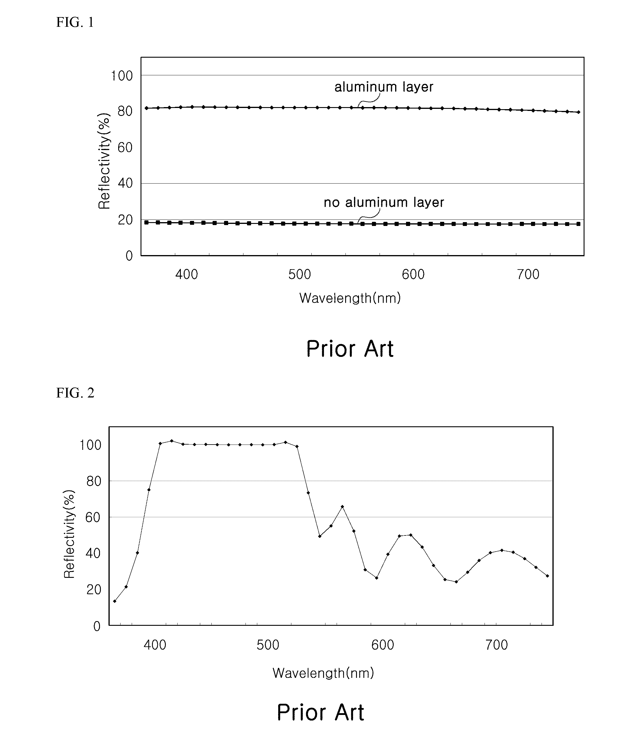
[0076]FIG. 8 is a simulation graph showing a change in reflectivity of a distributed Bragg reflector according to an incident angle. In this case, the distributed Bragg reflector is made by alternately stacking SiO2 and TiO2 on a glass substrate by 40 layers. The thickness of each layer is individually controlled to have the reflectivity of 99% or more over the entire area of 400 nm to 700 nm at an incident angle of 0°. Therefore, the thickness of the entire distributed Bragg reflector is 2.908 μm. Meanwhile, in the case of the substantially used light emitting diode chip, light incident at an incident angle of about 60° or more is totally reflected due to the difference in refractive index between the sapphire substrate (n equals about 1.78) and SiO2 (n equals about 1.48) and thus, the simulation for the incident angle of 60° or more is omitted. Meanwhile, the graph of FIG. 8 shows the entire visible area at the portion of 100% reflectivity (which was similarly shown in the graph o...


PUM


Abstract

Exemplary embodiments of the present invention disclose a light emitting diode chip including a substrate having a first surface and a second surface, a light emitting structure arranged on the first surface of the substrate and including an active layer arranged between a first conductive-type semiconductor layer and a second conductive-type semiconductor layer, a distributed Bragg reflector arranged on the second surface of the substrate, the distributed Bragg reflector to reflect light emitted from the light emitting structure, and a metal layer arranged on the distributed Bragg reflector, wherein the distributed Bragg reflector has a reflectivity of at least 90% for light of a first wavelength in a blue wavelength range, light of a second wavelength in a green wavelength range, and light of a third wavelength in a red wavelength range.

Description

CROSS-REFERENCE TO RELATED APPLICATIONS[0001]This application is a continuation-in-part of U.S. application Ser. No. 12 / 917,937, filed on Nov. 2, 2010, and claims priority from and the benefit of Korean Patent Application No. 10-2010-0013166, filed on Feb. 12, 2010, and Korean Patent Application No. 10-2010-0115347, filed on Nov. 19, 2010, which are hereby incorporated by reference for all purposes as if fully set forth herein.BACKGROUND OF THE INVENTION[0002]1. Field of the Invention[0003]Exemplary embodiments of the present invention relate to a light emitting diode chip and a method of fabricating the same, and to a light emitting diode chip having a distributed is Bragg reflector and a method of fabricating the same.[0004]2. Discussion of the Background[0005]A gallium nitride-based light emitting diode chip emitting blue or ultraviolet wavelength light may be used for various applications. In particular, various types of light emitting diode packages emitting mixed color light, ...

Claims


Application Information

Patent Timeline
IPC IPC(8): H01L33/46H01L33/08H01L33/22
CPCH01L27/153H01L33/46H01L33/0079H01L33/0093H01L2224/48091H01L2224/48247H01L2224/48257H01L2924/00014H01L33/0008H01L33/06H01L33/22H01L33/32H01L33/42H01L33/505H01L33/60H01L33/62H01L2933/0025H01L2933/0033H01L2933/0041H01L2933/0058
Inventor LEE, SUM GEUNJIN, SANG KISHIN, JIN CHEOLKIM, JONG KYULEE, SO RA
Owner SEOUL VIOSYS CO LTD
Why Eureka
Try Eureka