Spacer, and its manufacturing method

Inactive Publication Date: 2011-06-02
LENOVO INNOVATIONS LTD HONG KONG
View PDF12 Cites 17 Cited by
  • Summary
  • Abstract
  • Description
  • Claims
  • Application Information

AI Technical Summary

Benefits of technology

[0019]It is therefore an object of the present invention to overcome the issues of the above-described related techniques, and to provide a spacer as well as a manufacturing method thereof, which

Problems solved by technology

This may result in having a poor connection state, so that it is necessary to level the width of the clearance between the s

Method used


Image

  • Spacer, and its manufacturing method
  • Spacer, and its manufacturing method
  • Spacer, and its manufacturing method

Examples


Embodiment Construction

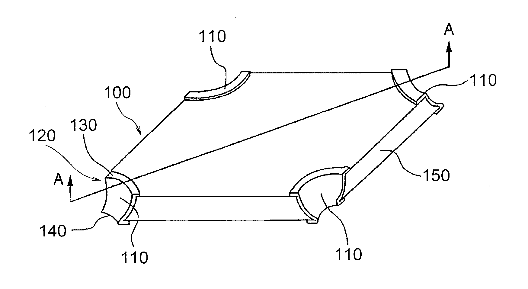
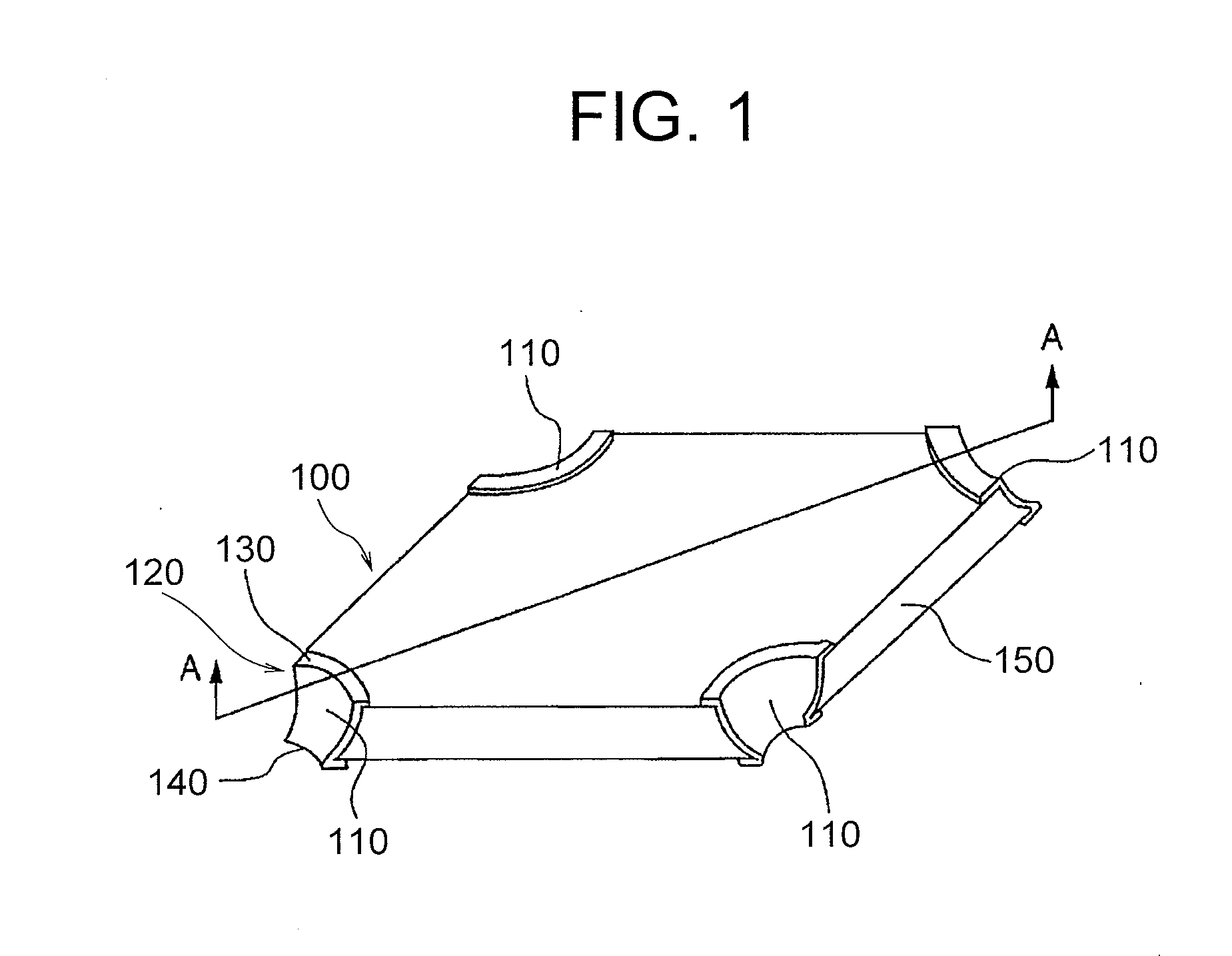
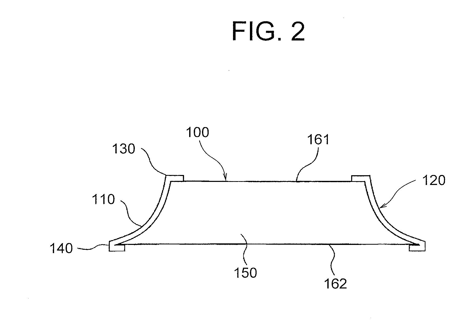
[0023]Hereinafter, preferable modes for embodying a spacer and a manufacturing method according to the present invention will be described in detail by referring to the accompanying drawings. In each drawing, each part may be illustrated in different scales from actual ones in some cases for simplifying the explanations of each part. For example, even though the thickness of metal terminals is normally 1 μtm or less, it is drawn in the thickness to be recognizable in the drawings.

[0024]The space of the exemplary embodiment is a spacer having an electric insulating base member and at least one solder guiding terminal. The surface of the base member is formed with a bottom face, a top face, and at least one side face. The bottom face and the top face do not come in contact with each other, and the side face is a face which is in contact with one of or both of the bottom face and the top face. The solder guiding terminal covers a part of the bottom face, a part of the top face, and a p...


PUM

PropertyMeasurementUnit
Angleaaaaaaaaaa
Widthaaaaaaaaaa
Areaaaaaaaaaaa

Abstract

Provided are a spacer capable of avoiding a poor connection due to the suction of solder when the clearance width between a soldered semiconductor device and a printed circuit board is made constant, and a manufacturing method for the spacer. The spacer includes an electrically insulating base member, and at least one solder guiding terminal. The base member has a bottom face, a top face and at least one side face, of which the bottom face and the top face are out of contact with each other whereas the side face contacts one or both the bottom face and the top face. The solder guiding terminal covers the bottom face partially, the top face partially, and the side face partially or wholly. A solder guiding face as the surface of a portion of the solder guiding terminal covering the side face is not normal to the bottom face.

Description

TECHNICAL FIELD[0001]The present invention relates to a spacer used for keeping the clearance width between soldering targets to be uniform when soldering and connecting a mounting board to an electronic component, such as a printed circuit board to a printed circuit board, a printed circuit board to a semiconductor circuit, and a printed circuit board to various devices, and also relates to a manufacturing method of the same.BACKGROUND ART[0002]In accordance with recent developments in technologies, power supply terminals and signal terminals in LSI (Large Scale Integrated Circuit) have been developed into multi-terminals due to the increasing information amount handled therewith and the tendency of having low voltage and high power. Methods for connecting LSI having several tens to several hundreds of terminals to a target board (printed circuit board, interposer, etc.) may be soldering using solder or the like, and adhesion using a conductive binder.[0003]With such connecting met...

Claims


Application Information

Patent Timeline
IPC IPC(8): H01L23/52H01L21/441H05K1/16H05K7/06B23K3/08B05D3/12
CPCH01G2/06H01L23/49805H01L2924/15311H01L23/49816H01L23/50H05K1/0231H05K1/141H05K1/145H05K3/3436H05K3/3442H05K3/403H05K2201/09181H05K2201/09836H05K2201/10378H05K2201/10636H05K2201/2036H01L2924/0002H01L2924/00Y02P70/50
Inventor MASUDA, KOICHIROMORI, TOORU
Owner LENOVO INNOVATIONS LTD HONG KONG
Why Eureka
Try Eureka