Luminescent display device

a technology of luminescent display and active matrix, which is applied in the direction of semiconductor devices, instruments, electrical apparatuses, etc., can solve the problems of reducing the lifetime of luminescent elements, increasing density, and less design flexibility, and achieves the effect of higher design flexibility

Active Publication Date: 2011-06-02
JOLED INC
View PDF21 Cites 46 Cited by
  • Summary
  • Abstract
  • Description
  • Claims
  • Application Information

AI Technical Summary

Benefits of technology

[0012]According to the present invention, it is possible to provide a luminescent display device with higher design flexibility by forming a capacitor without a region dedicated to the capacitor or a new region dedicated to the capacitor.

Problems solved by technology

With the above conventional technique, however, a region dedicated to the capacitor is formed, thereby causing a problem that when the number of capacitors or the capacitor area increases, the region for forming other elements becomes smaller, resulting in less design flexibility.
Alternatively, the luminescent region becomes smaller, leading to an increase in the density of the current flowing in the luminescent element, thereby reducing the lifetime of the luminescent element.

Method used


Image

  • Luminescent display device
  • Luminescent display device
  • Luminescent display device

Examples


embodiment 1

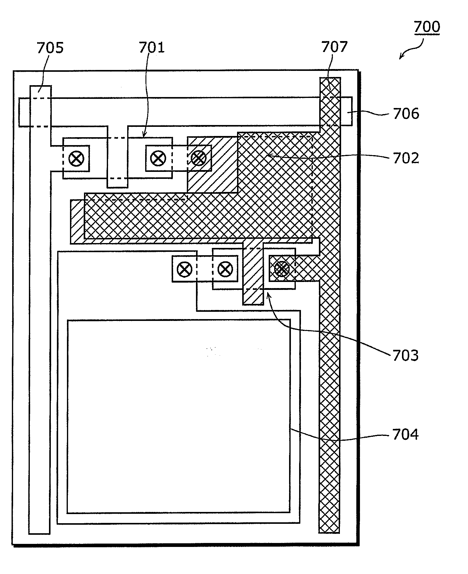
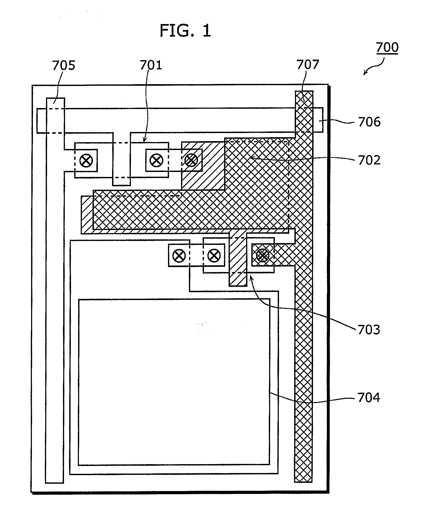
[0050]The luminescent display device according to Embodiment 1 includes a driving transistor and a capacitor, and the gate electrode of the driving transistor is one of two capacitor electrodes constituting the capacitor. Thus, the capacitor is formed in a region which is above the driving transistor and which includes the gate electrode of the driving transistor.

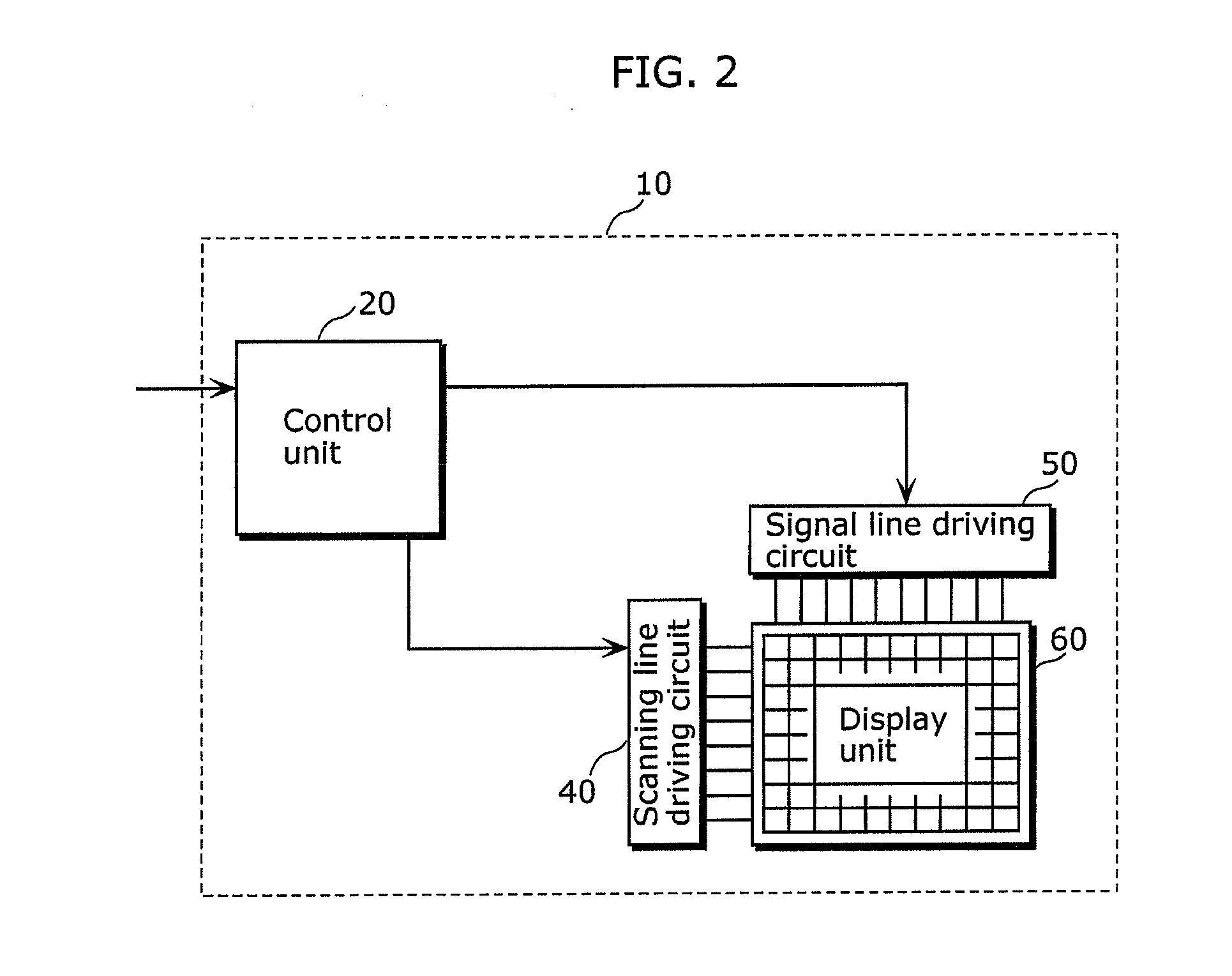
[0051]FIG. 2 is a block diagram showing an electrical structure of a luminescent display device 10 according to Embodiment 1. The luminescent display device 10 in FIG. 2 at least includes a control circuit 20, a scanning line driving circuit 40, a signal line driving circuit 50, and a display unit 60.

[0052]FIG. 3 shows a circuit structure of a luminescent pixel 100 included in the display unit 60 according to Embodiment 1. The luminescent pixel 100 in FIG. 3 includes a switching transistor 101, a capacitor 102, a driving transistor 103, an organic EL element 104, a signal line 105, a scanning line 106, a higher-voltage-side...

embodiment 2

[0122]The luminescent display device according to Embodiment 2 includes a switching transistor, a driving transistor, and a capacitor, and the gate electrode of the switching transistor is one of two capacitor electrodes constituting the capacitor. Thus, the capacitor is formed in the region above the switching transistor.

[0123]The luminescent display device according to Embodiment 2 is different from the luminescent display device 10 according to Embodiment 1 in circuit structure of each luminescent pixel included in the display unit and in arrangement of elements constituting each luminescent pixel. In other words, the luminescent display device according to Embodiment 2 has the same electrical structure as that of the luminescent display device 10 according to Embodiment 1 shown in FIG. 2. Thus, the description of the electrical structure of the luminescent display device according to Embodiment 2 is omitted, and the following description centers on the circuit structure of each ...


PUM


Abstract

A luminescent display device includes a substrate and a thin-film transistor above the substrate. The thin-film transistor includes a semiconductor layer, a gate insulating film on the semiconductor layer, a gate electrode on the gate insulating film, a source electrode, and a drain electrode. The luminescent display device further includes an interlayer insulating film on the gate electrode, a first capacitor electrode on the interlayer insulating film in a region above the gate electrode, and a luminescent element configured to be driven by a driver to produce luminescence. The driver includes the thin-film transistor, and the first capacitor electrode and the gate electrode constitute a capacitor.

Description

CROSS REFERENCE TO RELATED APPLICATION[0001]This is a continuation application of PCT Application No. PCT / JP2009 / 006415, filed on Nov. 27, 2009, designating the United States of America, the disclosure of which, including the specification, drawings, and claims, is incorporated herein by reference in its entirety.BACKGROUND OF THE INVENTION[0002]1. Field of the Invention[0003]The present invention relates to luminescent display devices, and particularly to an active-matrix luminescent display device which includes a luminescent element and a driving circuit having a capacitor and a thin-film transistor.[0004]2. Description of the Related Art[0005]Conventionally, there is an active development of luminescent display devices, such as organic electroluminescent elements (hereinafter abbreviated as organic EL elements), in which luminescent elements that control the luminance using an electric current are two-dimensionally arranged. In particular, there is an ongoing development of acti...

Claims


Application Information

Patent Timeline
Patent Type & Authority Applications(United States)
IPC IPC(8): G09G3/30
CPCH01L27/3265H01L27/1255G09G3/3233H10K59/1216H01L27/1214H01L27/13H01L29/41733
Inventor ONO, SHINYA
Owner JOLED INC
Why Eureka
Try Eureka