

Image sensor and method of manufacturing the same
- Summary
- Abstract
- Description
- Claims
- Application Information
AI Technical Summary
Benefits of technology
Problems solved by technology
Method used
Image

Examples
embodiment 1
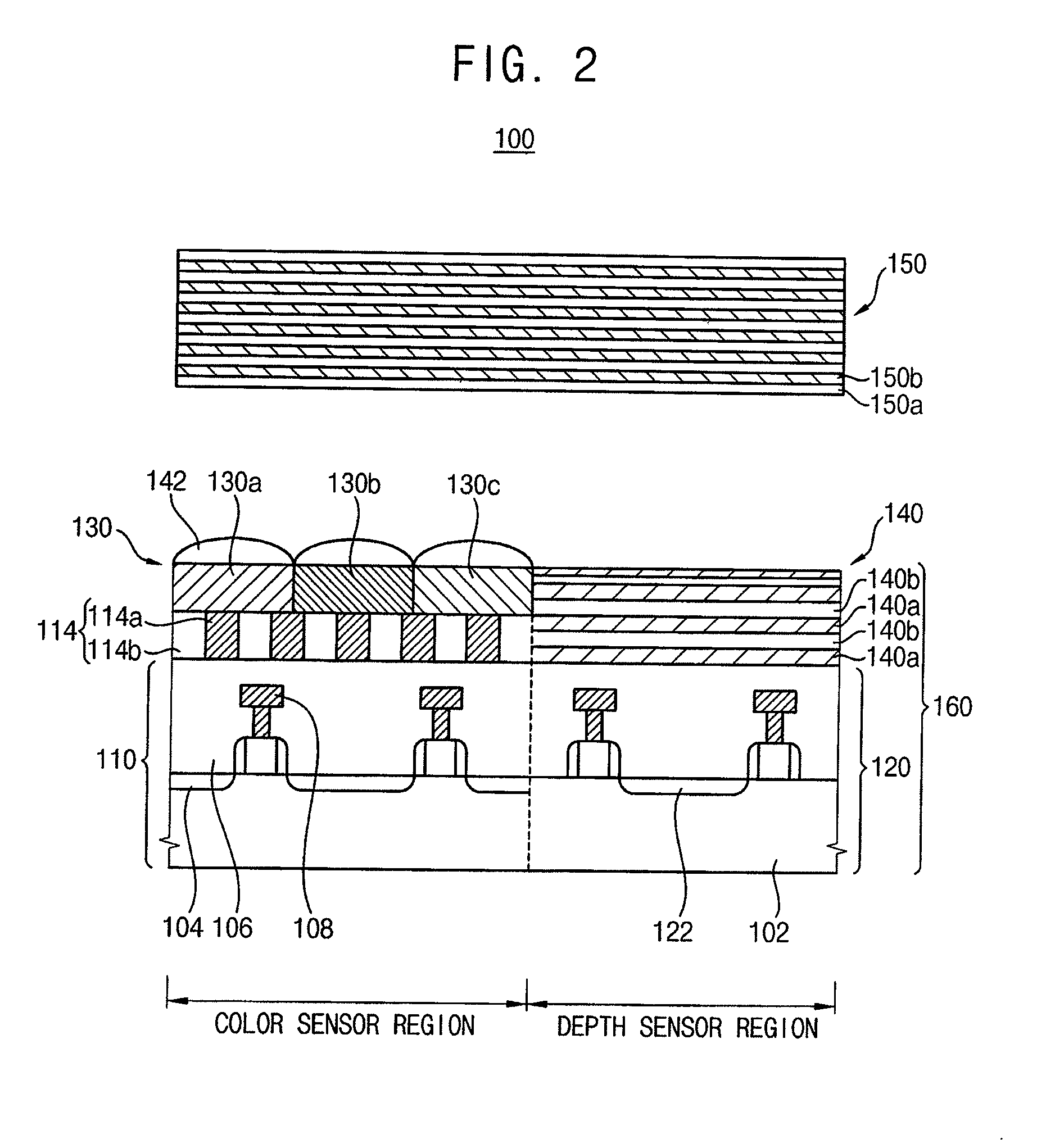
[0054]FIG. 1 is a diagram illustrating a three-dimensional color image sensor in accordance with a first embodiment of the present inventive concept. FIG. 2 is a cross-sectional view of a three-dimensional color image sensor illustrated in FIG. 1. FIG. 3 is a graph illustrating spectrum characteristics of filters included in a three-dimensional color image sensor illustrated in FIG. 1. FIG. 4 is a perspective view of a near-infrared cut filter included in a three-dimensional color image sensor illustrated in FIG. 1. FIG. 5 is a diagram illustrating an arrangement of filters included in a three-dimensional color image sensor illustrated in FIG. 1.
[0055]Referring to FIGS. 1 and 2, a three-dimensional color image sensor 100 includes an image sensor 160 and a rejection filter 150.
[0056]The image sensor 160 includes color sensors 110 and depth sensors 120. The image sensor 160 may further include different filters 114, 130 and 140 respectively formed on the color sensors 110 and the dept...
embodiment 2
[0119]FIG. 13 is a cross-sectional view of a three-dimensional color image sensor in accordance with a second embodiment of the present inventive concept.
[0120]As illustrated in FIG. 13, a three-dimensional color image sensor according to the second embodiment is substantially similar to the three-dimensional color image sensor according to the first embodiment except for the arrangement of filters on color sensors 110. Unlike the first embodiment, a NIR cut filter 114 may be formed on a color filter 130 in the second embodiment.
[0121]FIGS. 14 and 15 are cross-sectional views for illustrating a method of manufacturing a three-dimensional color image sensor illustrated in FIG. 13.
[0122]Referring to FIG. 14, color sensors 110 and depth sensors 120 are formed on a substrate.
[0123]A multi-layer structure is formed by alternately stacking a silicon layer 140a and a silicon oxide layer 140b on the color sensors 110 and the depth sensors 120. A NIR band pass filter 140 may be formed on the...
embodiment 3
[0128]FIG. 16 is a cross-sectional view of a three-dimensional color image sensor in accordance with a third embodiment of the present inventive concept. FIG. 17 is a perspective view of a NIR cut filter included in a three-dimensional color image sensor illustrated in FIG. 16.
[0129]As illustrated in FIG. 16, a three-dimensional color image sensor according to the third embodiment is substantially similar to the three-dimensional color image sensor according to the first embodiment except for a NIR cut filter 116 on color sensors 110.
[0130]Referring to FIGS. 16 and 17, the NIR cut filter 116 formed on the color sensors 110 may a photonic crystal structure where at least two materials having different refractive indexes are periodically arranged.
[0131]In the third embodiment, the NIR cut filter 116 may include first patterns 116b that are periodically arranged, and a second pattern 116a that fills spaces between the first patterns 116b with a material having a refractive index differ...
PUM
 Abstract
Description
Claims
Application Information