Capacitive touch device structure

Inactive Publication Date: 2011-06-09
J TOUCH CORPORATION
View PDF2 Cites 37 Cited by
  • Summary
  • Abstract
  • Description
  • Claims
  • Application Information

AI Technical Summary

Benefits of technology

[0015]After the first transparent substrate and the second transparent substrate are attached by an adhesive layer, the picture layer is covered at the periphery of the lower surface of the first transparent substrate, whose interior hollow area is the covering area of the first transparent conductive thin film, and the first circuits are installed within the range area of the picture layer, and the intersection of the picture layer and the first transparent conductive thin film is near the electric connecting positions of the first sensing electrodes and the first circuits, so that the

Problems solved by technology

As a result, the thickness of the touch panel still cannot be reduced effectively.
Although this patented technology

Method used


Image

  • Capacitive touch device structure
  • Capacitive touch device structure
  • Capacitive touch device structure

Examples


Example

[0023]The technical characteristics of the present invention will become apparent with the detailed description of the preferred embodiments and the illustration of the related drawings.

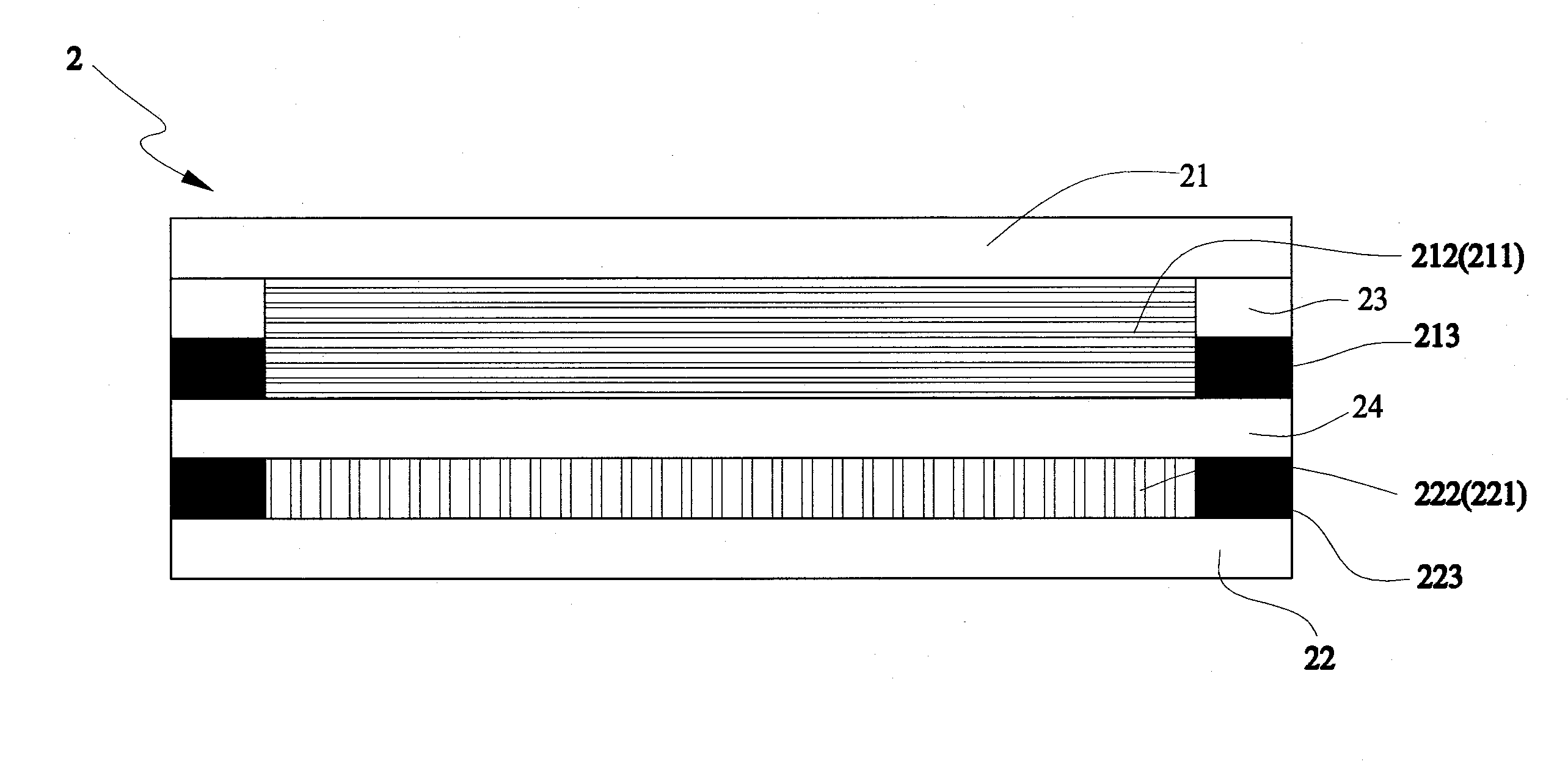
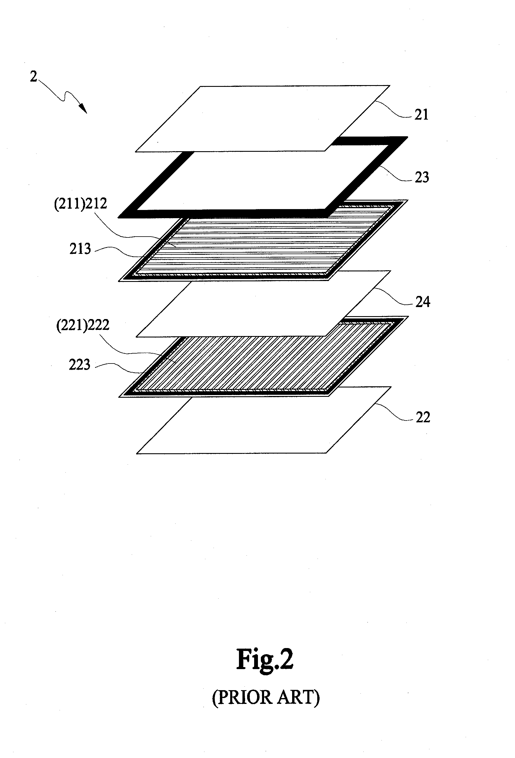
[0024]With reference to FIGS. 2 and 3 for an exploded view and a cross-sectional view of a capacitive touch device structure in accordance with a preferred embodiment of the present invention, the capacitive touch device structure includes a capacitive touch device 2 comprising a first transparent substrate 21, a first transparent conductive thin film 211, a second transparent substrate 22, a second transparent conductive thin film 221, a picture layer 23 and an adhesive layer 24 for laminating the transparent substrates 21, 22.

[0025]The first transparent substrate 21 is composed of a group of transparent plate made of a material selected from glass, polyethylene terephthalate (PET), polycarbonate (PC), polyethylene (PE), polyvinyl Chloride (PVC), polypropylene (PP), polystyrene (PS), polymethylmetha...


PUM


Abstract

A capacitive touch device structure includes a first transparent substrate, a second transparent substrate, a picture layer at the periphery of a lower surface of the first transparent substrate, first and second transparent conductive thin films formed on corresponding surfaces of the two transparent substrates respectively, a plurality of first and second circuits, and an adhesive layer for laminating the first and second transparent substrates. After the corresponding surfaces of the capacitive touch device are attached, the first or second transparent conductive thin film and the first or second circuit are considered to be in the same plane, so as to achieve the effects of reducing the thickness of the capacitive touch device, improving the light transmittance effectively, minimizing the number of layers of the first or second transparent conductive thin film and the first or second circuit, simplifying the manufacturing process and improving the yield rate.

Description

BACKGROUND OF THE INVENTION[0001]1. Field of the Invention[0002]The present invention relates to a touch device, and more particularly to a capacitive touch device structure capable of reducing the thickness, improving the light transmittance, and simplifying the manufacturing process of a touch panel.[0003]2. Description of the Related Art[0004]Touch panel is generally divided into resistive, capacitive, ultrasonic, and optical (infrared) touch panel. Among these touch panels, the resistive touch panel is the most commonly used one, and the capacitive touch panel is the second commonly used one. Although the capacitive touch panel comes at a higher price, it has the advantages of high water resistance, scratch resistance and light transmittance as well as wide applicable temperature range. Therefore, the capacitive touch panel is introduced and used in the market of small touch panels as the technology matures.[0005]With reference to FIG. 1 for a schematic view of a conventional to...

Claims


Application Information

Patent Timeline
IPC IPC(8): G06F3/044
CPCG06F3/044G06F3/0446G06F3/0445G06F3/04164G06F1/1613G06F1/1626G06F1/1643G06F2203/04111
Inventor YEH, YU-CHOUJAN, HSIAO-SHUNTENG, CHIEH-JEN
Owner J TOUCH CORPORATION
Why Eureka
Try Eureka