Semiconductor light source apparatus and lighting unit

a technology of semiconductor light source and light source apparatus, which is applied in the direction of lighting and heating apparatus, semiconductor devices for light sources, instruments, etc., can solve the problems of reducing the excitation intensity, affecting the brightness of semiconductor light source apparatus, and tarnishing of transparent resin

Active Publication Date: 2011-06-23
STANLEY ELECTRIC CO LTD
View PDF4 Cites 177 Cited by
  • Summary
  • Abstract
  • Description
  • Claims
  • Application Information

AI Technical Summary

Benefits of technology

[0024]In the immediately above-described exemplary semiconductor light source apparatuses, a color tone of an illumination light having a large amount of light intensity can be adjusted by changing the distance between the intersection of the optical axis of the semiconductor light source and the mounting surface and the rotation axis of the radiating substrate. In addition, the blue phosphor layer can be eliminated by replacing the ultraviolet light-emitting device with a blue light-emitting device. In this case, the semiconductor light source apparatus can efficiently use blue light that is not excited by the red and green phosphor layers with a cutout section, which exposes a part of the radiating substrate from the red and green phosphor layers.
[0025]According to the above-described exemplary semiconductor light source apparatus, the color tone of light emitted from the semiconductor light source apparatus can be adjusted by the moving module for changing the distance between the intersection of the optical axis of the semiconductor light source and the mounting surface and the rotation axis of the radiating substrate because the light source apparatus can vary a ratio of mixing lights for white light according to the distance. Moreover, a high power semiconductor light-emitting device can be used under the large current as the light source due to a radiating effective by a rotation of the radiating substrate. Thus, the semiconductor light source apparatus can adjust a color tone of an illumination light having a large amount of light intensity.

Problems solved by technology

However, because heat occurs in the phosphor layer due to the large current, the transparent resin can be tarnished.
Because the transparent resin is mixed in the phosphor layer, the tarnish of the transparent resin results in absorption of a part of light excited by the phosphor layer, and therefore may cause a reduction of the excitation intensity.
Therefore, because the tarnish of the transparent resin and the reduction of the fluorescent intensity cause a reduction of a light intensity in semiconductor light source apparatuses that include a phosphor layer, it is difficult to improve the brightness of the semiconductor light source apparatuses by simply flowing a large current.
The reflected light may cause a reduction of light use efficiency.
However, because the semiconductor light-emitting device 95 also generates heat, a radiating efficiency of the semiconductor light source apparatus may not be high.
However, because the phosphor layer includes a phosphor particle in a transparent resin, when a high power light source device is used for the semiconductor light source apparatus for many years, a degradation of the transparent resin may occur.

Method used


Image

  • Semiconductor light source apparatus and lighting unit
  • Semiconductor light source apparatus and lighting unit
  • Semiconductor light source apparatus and lighting unit

Examples


second embodiment

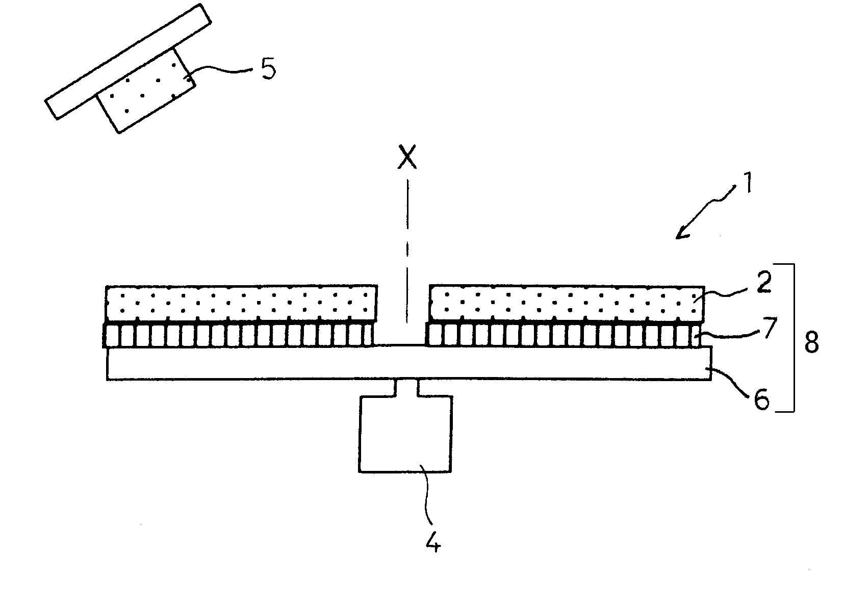
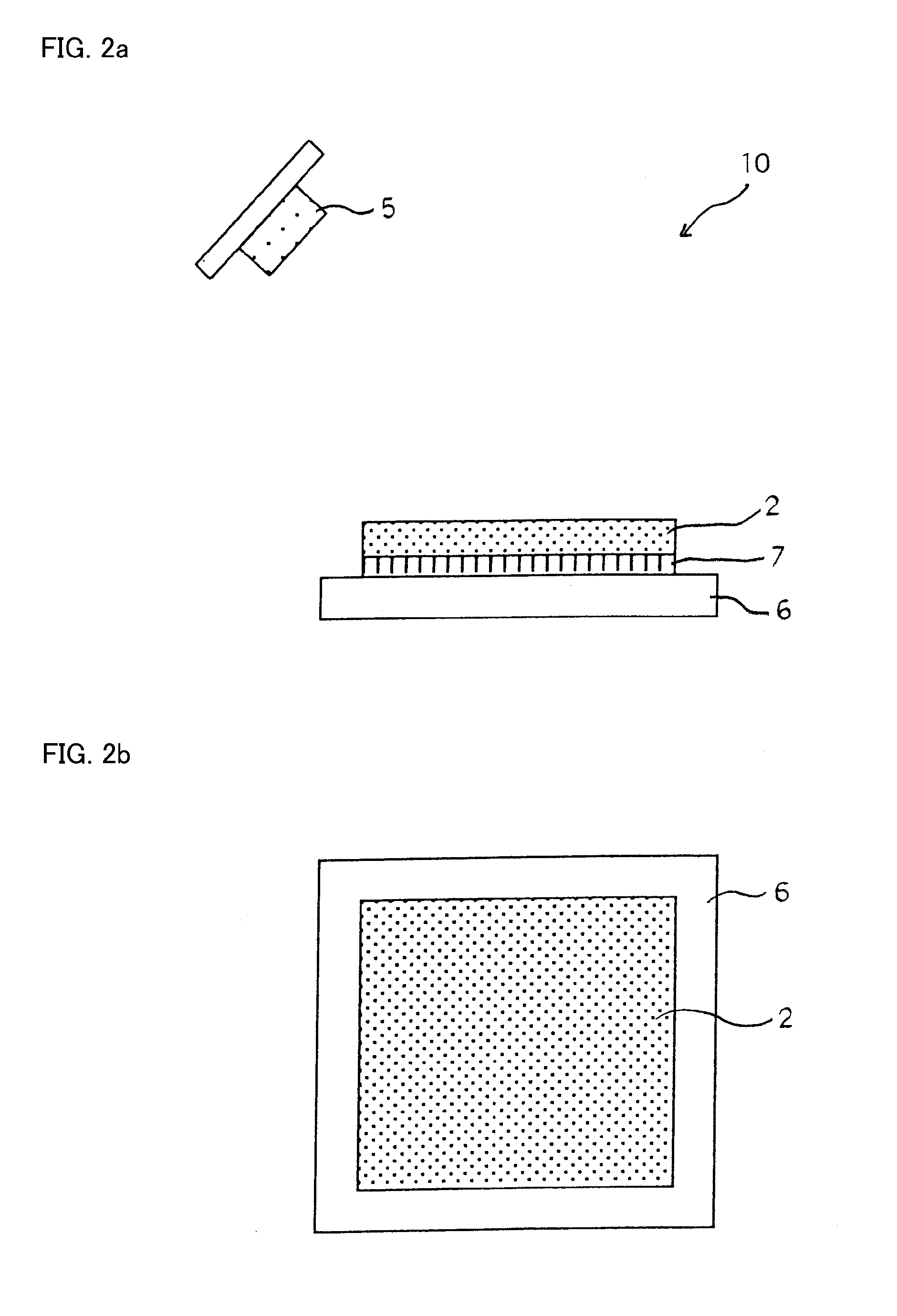
[0074]FIG. 4 is a schematic structural view showing a second exemplary embodiment of a semiconductor light source apparatus of the disclosed subject matter. FIGS. 5a and 5b are schematic top and front views showing a phosphor wheel of the second exemplary semiconductor light source apparatus. The semiconductor light source apparatus 1 in the second embodiment can include a rotary phosphor wheel 8 including the phosphor layer 2 and the radiating substrate 6.

first embodiment

[0075]Accordingly, the semiconductor light source apparatus 1 can further improve the radiating efficiency of the phosphor layer 2 as compared with the semiconductor light source apparatus 10 of the The semiconductor light source apparatus 1 can include: a motor 4 having a rotation axis; the phosphor layer 2; the radiating substrate 6 having a rotation axis X being connected to the rotation axis of the motor 4 so that the phosphor layer 2 can be rotated at a substantially right angle with the rotation axis X of the radiating substrate 6 by the motor 4; and a semiconductor light source 5 emitting ultraviolet light or blue light.

[0076]In this case, when the phosphor layer 2 includes the yellow phosphor wavelength-converting the blue light into yellow light, the semiconductor light source apparatus 1 can emit substantially white light due to an additive color mixture using light excited by the yellow phosphor and a part of the blue light that is not excited by the yellow phosphor. Whe...

third embodiment

[0090]A phosphor wheel 11 of the third embodiment can include a red phosphor layer 2a formed in a fan shape; a green phosphor layer 2b formed in a fan shape; a blue phosphor layer 2c formed in a fan shape; a first boundary straight line 3a located between the red and green phosphor layers 2a and 2b; a second boundary straight line 3b located between the green and blue phosphor layers 2b and 2c; a boundary curved line 3c located between the blue and red phosphor layers 2c and 2a; and the semiconductor light source 5 having an optical axis Y that emits ultraviolet light.

[0091]The boundary curved line 3c can divide the red phosphor layer 2a and the blue phosphor layer 2c so that a ratio of an imaginary arc (that is part of an imaginary circle) located on (or travelling through) the red phosphor layer 2a to an imaginary arc located on (or travelling through) the blue phosphor layer 2c becomes larger as an intersection of the arc and the boundary curved line 3c approaches the rotation ax...


PUM

PropertyMeasurementUnit
angleaaaaaaaaaa
angleaaaaaaaaaa
light-emitting wavelengthaaaaaaaaaa

Abstract

A semiconductor light source apparatus can emit various color lights having high brightness. The semiconductor light source apparatus can include a radiating substrate, at least one phosphor layer disposed on the radiating substrate and a semiconductor light source. The at least one phosphor layer can be composed of at least one of a glass phosphor and a phosphor ceramic and can include at least one of a red phosphor, a green phosphor and a blue phosphor. The light source can be located adjacent the phosphor layer so that light having high brightness emitted from the light source can be efficiently reflected on the radiating substrate via the at least one phosphor layer. Thus, the disclosed subject matter can provide a semiconductor light source apparatus that can emit various color lights having high brightness and a lighting unit using the light source apparatus, which can be used for general lighting, etc.

Description

[0001]This application claims the priority benefit under 35 U.S.C. §119 of Japanese Patent Application No. 2009-286397 filed on Dec. 17, 2009 and Japanese Patent Application No. 2009-287559 filed on Dec. 18, 2009, both of which are hereby incorporated in their entireties by reference.BACKGROUND[0002]1. Field[0003]The presently disclosed subject matter relates to a semiconductor light source apparatus and a lighting unit using the semiconductor light source apparatus, and more particularly to a high power semiconductor light source apparatus including a phosphor layer that can prevent a reduction of brightness caused by thermal quenching and a lighting unit that can also emit various color lights having a large amount of light intensity in order to be able to be used for general lighting, a stage light, a street light, a projector, etc.[0004]2. Description of the Related Art[0005]Semiconductor light source apparatuses that emit various color lights by combining a phosphor layer with ...

Claims


Application Information

Patent Timeline
Patent Type & Authority Applications(United States)
IPC IPC(8): F21V9/16
CPCF21K9/56F21V7/22G03B21/204F21Y2101/02F21Y2101/025F21V9/16F21K9/64F21Y2115/30F21Y2115/10F21V9/45F21V9/32F21V9/38F21V13/08F21V7/30
Inventor MIYAKE, YASUYUKI
Owner STANLEY ELECTRIC CO LTD
Why Eureka
Try Eureka