
Photovoltaic cell manufacturing method

a photovoltaic cell and manufacturing method technology, applied in the field of photovoltaic cell manufacturing method, can solve the problems of large amount of energy spent on manufacturing silicon single crystal ingots, cost significantly increases, and high manufacturing cost of photovoltaic cells in which silicon single crystal is used, so as to reduce the number of removal processes, suppress adverse effects, and remove the region at which structural defects exist.

Inactive Publication Date: 2011-06-23
ULVAC INC
View PDF6 Cites 11 Cited by
  • Summary
  • Abstract
  • Description
  • Claims
  • Application Information

AI Technical Summary

Benefits of technology

[0038]According to the above-described invention (1), one repair line is formed between the structural defect and the connection portion of the first electrode layer and the second electrode layer and is formed at the region α including the portion at which the semiconductor layer is in contact with the substrate; and, by using the repair line, at least two of the other repair lines, and the scribing line, it is possible to reliably remove and separate the region at which the structural defect exists.
[0039]Additionally, a region which is removed or separated from a normal region becomes lower than ever before. Since it is only necessary to remove two layers of the semiconductor layer and the second electrode layer with a laser in the repair line, it is possible to reduce the number of removal processes with a laser, which is lower than ever before, and suppressing an adverse affect to a normal region of a photovoltaic cell.
[0040]Therefore, it is possible to manufacture a photovoltaic cell having a high level of photoelectric conversion efficiency without a structural defect.
[0041]According to the above-described inventions (2) and (3), it is possible to narrow down the region further which is to be removed or separated from the normal amount region more than that of the above-described invention (1), and it is possible to repair the defect portion without significant degradation of the characteristics of a photovoltaic cell and without resulting in disfigurement.
[0042]Because of this, it is possible to manufacture a photovoltaic cell having a high level of photoelectric conversion efficiency without a structural defect.

Problems solved by technology

However, in the photovoltaic cell in which the silicon single crystal is utilized, a silicon single crystal ingot is sliced, the sliced silicon wafer that is obtained is used in the photovoltaic cell; therefore, a large amount of energy is spent for manufacturing the silicon single crystal ingot.
Consequently, the manufacturing cost of the photovoltaic cell in which the silicon single crystal is utilized is high.
Specifically, at the moment, in a case of realizing a photovoltaic cell having a large area which is placed out doors or the like, when the photovoltaic cell is manufactured by use of a silicon single crystal, the cost considerably increases.
In the amorphous silicon photovoltaic cell that is provided with a photoelectric converter having the upper electrode, the lower electrode, and the semiconductor film as described above, if each of the layers having a large area is only uniformly formed on the substrate, there is a problem in that the difference in the electrical potentials is small and there is a problem of resistance.
However, in the amorphous silicon photovoltaic cell having the foregoing structure, it is known that several structural defects occur during a manufacturing step therefor.
As described above, in the photoelectric converter, when structural defects occur such that the upper electrode and the lower electrode are locally short-circuited with the semiconductor film interposed therebetween, the defects cause malfunction such that power generation voltage or photoelectric conversion efficiency are degraded.
Furthermore, there is a concern in that a photoelectric converter of a photovoltaic cell is damaged.

Method used


Image

  • Photovoltaic cell manufacturing method
  • Photovoltaic cell manufacturing method
  • Photovoltaic cell manufacturing method

Examples


Embodiment Construction

[0056]Hereinafter, an embodiment of a photovoltaic cell manufacturing method related to the present invention will be described with reference to drawings.

[0057]The embodiment is specifically explained for appropriate understanding the scope of the present invention, and does not limit the present invention unless otherwise specified.

[0058]Also, for convenience, the drawings used in below explanation may indicate a portion that becomes relevant part of the present invention in a enlarged state for appropriate understanding the features of the present invention, and the size of each constituent element is not limited to the same size as a practical element.

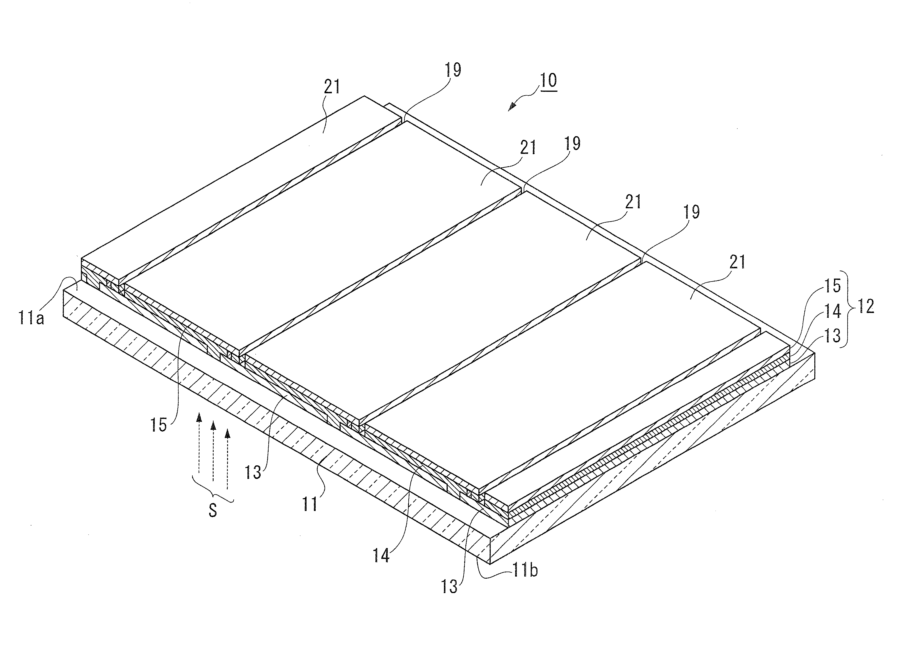
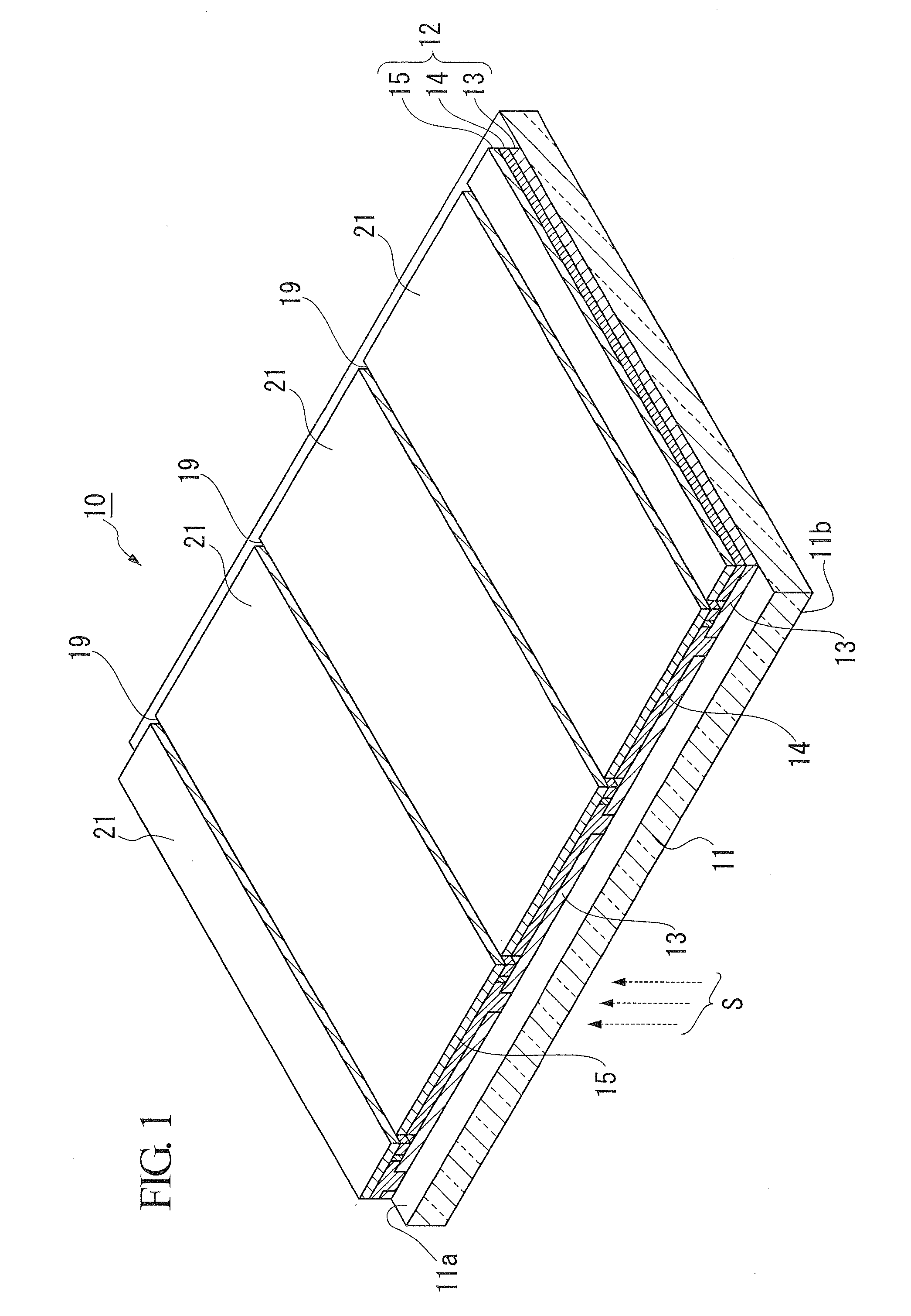
[0059]FIG. 1 is an enlarged perspective view showing an example of a main section of an amorphous silicon type photovoltaic cell which is manufactured by a photovoltaic cell manufacturing method of the present invention.

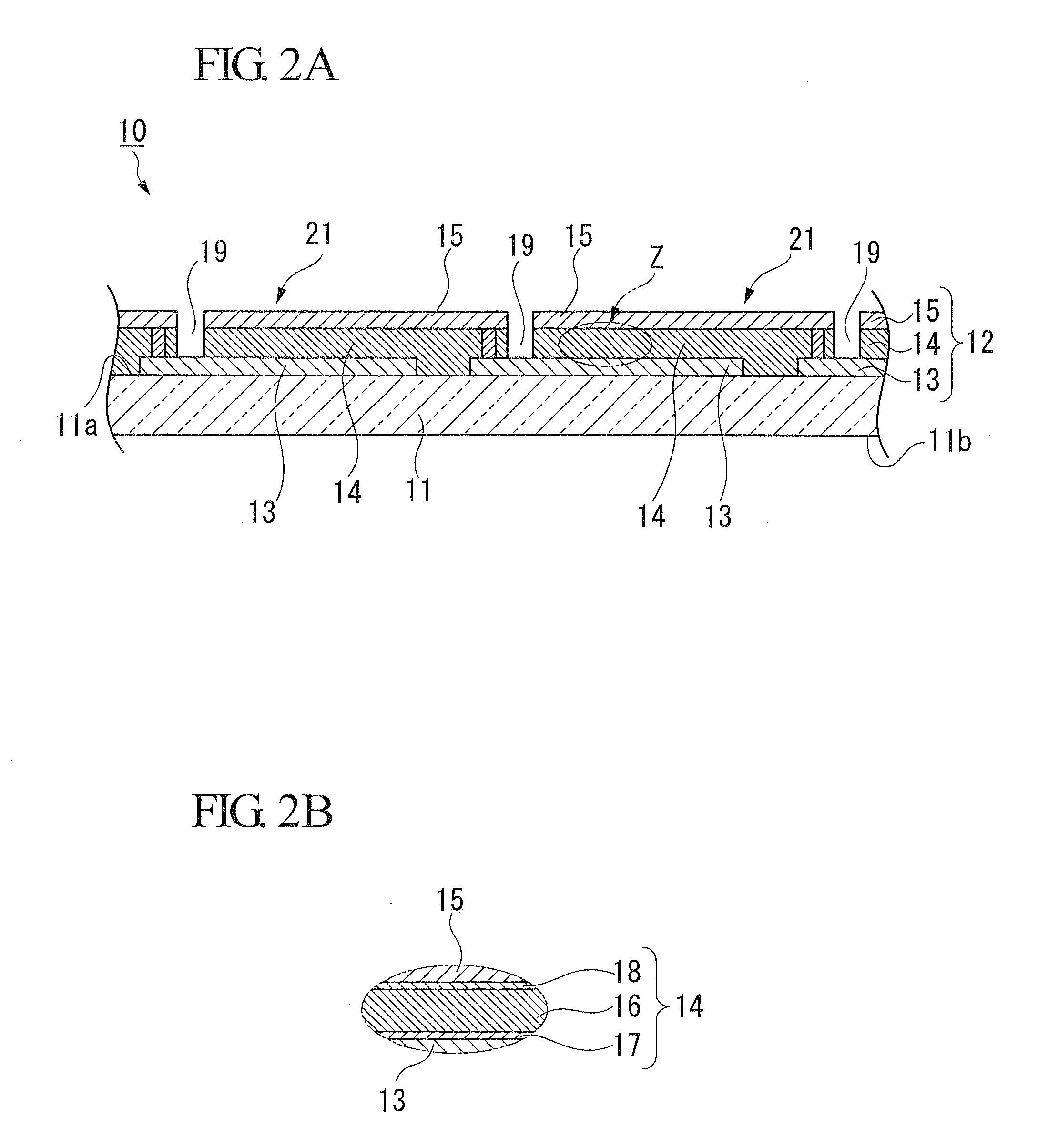
[0060]In addition, FIG. 2A is a cross-sectional view partially showing a layered structure of the photovoltaic ce...


PUM


Abstract

The present invention provides a photovoltaic cell manufacturing method, the photovoltaic cell including: a photoelectric converter in which at least a first electrode layer, a semiconductor layer, and a second electrode layer are stacked in layers in this order being formed on a face of a substrate; and a connection portion of the first electrode layer and the second electrode layer, the photoelectric converter having a plurality of compartment elements which are electrically separated by a predetermined size using scribing lines at which the semiconductor layer and the second electrode layer are removed, adjacent compartment elements being electrically connected to each other, the photovoltaic cell manufacturing method comprising: a defect region specifying step in which a region at which the structural defect exists is specified in the photoelectric converter; and a repairing step in which at least three repair lines in which the semiconductor layer and the second electrode layer are removed are formed by irradiating the photoelectric converter with a laser, the region at which the structural defect exists is surrounded by at least three repair lines described above and one of the scribing lines, and the structural defect is removed or separated off, wherein one of at least three repair lines described above are formed at a region between the structural defect and the connection portion and at a region α including a contact portion of the semiconductor layer and the substrate in the photoelectric converter.

Description

BACKGROUND OF THE INVENTION[0001]1. Field of the Invention[0002]The present invention relates to a photovoltaic cell manufacturing method.[0003]Particularly, the present invention relates to a photovoltaic cell manufacturing method which forms repair line by removing a semiconductor layer and a second electrode layer with a laser, and can reliably remove and separate a structural defect region from a normal region using the repair line and a scribing line.[0004]Additionally, in details, the present invention relates to a photovoltaic cell manufacturing method which can minimize degradation of the photoelectric conversion efficiency by minimizing the area that is used for removing and separating a structural defect region from a normal region.[0005]This application claims priority from Japanese Patent Application No. 2008-222171 filed on Aug. 29, 2008, the contents of which are incorporated herein by reference in their entirety.[0006]2. Background Art[0007]In recent years, in view of...

Claims


Application Information

Patent Timeline
Patent Type & Authority Applications(United States)
IPC IPC(8): H01L31/18
CPCH01L31/186H01L31/046H01L31/208Y02E10/50Y02P70/50
Inventor YAMAMURO, KAZUHIROYUYAMA, JUNPEIYAMANE, KATSUMI
Owner ULVAC INC
Learn More