Liquid Crystal Display Panel and Liquid Crystal Display

Active Publication Date: 2011-06-30
KUSN INFOVISION OPTOELECTRONICS
View PDF1 Cites 12 Cited by
  • Summary
  • Abstract
  • Description
  • Claims
  • Application Information

AI Technical Summary

Benefits of technology

[0019]As can be seen from the present invention, it is not necessary to form the bumps or the slits in the liquid crystal display panel by using the masks as in the conventional VA technologies, thereby reducing the complexity of the manufacture process of the li

Problems solved by technology

In the conventional VA technologies, it is necessary to add a masking technology in a manufacture process of the CF substrate, so as to form the bumps or the slits, which increases the complexity of the manufacture process of the liquid crystal display panel, and decreases the yield of products.
Moreover, since the liquid crystal molecules at the bumps are vertical to the surface of the bumps, light leakage can not be avoided when the liquid crystal display panel i

Method used


Image

  • Liquid Crystal Display Panel and Liquid Crystal Display
  • Liquid Crystal Display Panel and Liquid Crystal Display
  • Liquid Crystal Display Panel and Liquid Crystal Display

Examples


first embodiment

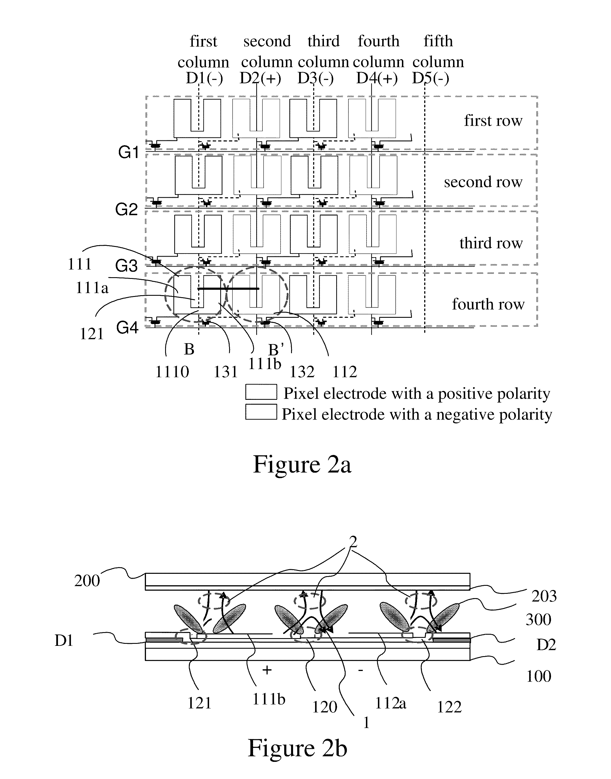
[0028]FIG. 2a is a schematic diagram illustrating structure of a portion of a liquid crystal display panel according to the present invention, which indicates a display effect of a column inversion, and FIG. 2b is a sectional view along a B-B′ direction shown in FIG. 2a. For clarity, FIG. 2a shows structure of a portion of a lower substrate facing to a liquid crystal layer in the liquid crystal display panel. The liquid crystal display panel in the embodiment includes a first substrate 100 and a second substrate 200 which are opposite (respectively correspond to a lower substrate and an upper substrate), and a liquid crystal layer 300 sealed between the two substrates. As shown in FIG. 2a, the lower substrate includes a plurality of scanning lines extending along a row direction and a plurality of data lines extending along a column direction. Only four scanning lines represented as G1, G2, G3 and G4 and five data lines represented as D1, D2, D3, D4 and D5 are shown in FIG. 2a. The ...

second embodiment

[0034]FIG. 3 is a schematic diagram illustrating structure of a portion of a liquid crystal display panel which indicates a display with a dot inversion. The liquid crystal display panel in the embodiment includes a first and a second substrates which are opposite (respectively correspond to a lower substrate and an upper substrate), and a liquid crystal layer 300 sealed between the two substrates. For clarity, FIG. 3 also shows structure of a portion of the lower substrate facing to the liquid crystal layer. As shown in FIG. 3, the lower substrate includes a plurality of scanning lines extending along the row direction and a plurality of data lines approximately extending along the column direction. Only four scanning lines represented as G1, G2, G3 and G4 and five data lines represented as D1, D2, D3, D4 and D5 are shown in FIG. 3. Preferably, the plurality of data lines approximately extending along the column direction has zigzag structures. The intersection of any two adjacent...

third embodiment

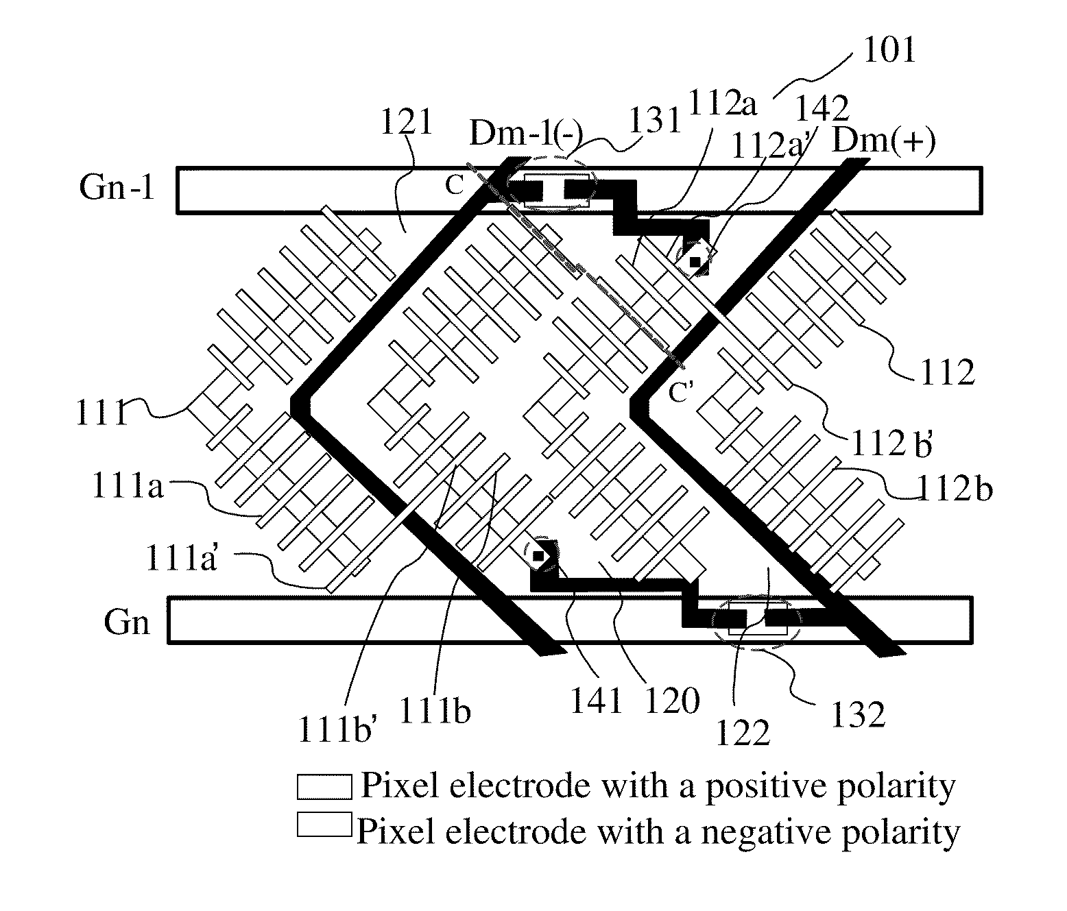
[0037]FIGS. 4a and 4b are respectively a plan schematic diagram illustrating structure of a portion of a liquid crystal display panel and a sectional view along a C-C′ direction of the liquid crystal display panel according to the present invention. Similarly, the liquid crystal display panel in this embodiment includes a first substrate and a second substrate which are opposite (respectively correspond to a lower substrate and an upper substrate), and a liquid crystal layer sealed between the two substrates. For clarity, FIG. 4a shows the structure of a portion of the lower substrate facing to the liquid crystal layer. As shown in FIG. 4a, the lower substrate includes a plurality of scanning lines extending along a row direction and a plurality of data lines approximately extending along a column direction. Only two adjacent scanning lines represented as Gn−1 and Gn and two adjacent data lines represented as Dm−1 and Dm are shown in FIG. 4a. The intersection of the scanning lines G...


PUM


Abstract

A liquid crystal display panel includes a first and second substrates which are opposite, and further includes scanning lines, data lines, pixel electrodes and switches, intersection of two adjacent scanning lines and data lines forming a pixel region. The pixel electrodes are disposed in pixel regions. Each pixel electrode crosses one data line and includes a first and second sub-pixel electrodes which are electrically connected to each other; the first and second sub-pixel electrodes are arranged on two sides of the data line; there is a gap between the first and second sub-pixel electrodes, and the data line is configured in the gap. A problem that conventional liquid crystal display panel has a complex manufacture process, leaks light at a dark state and has a low penetrability can be solved, thereby improving yield of the products.

Description

FIELD OF THE INVENTION[0001]The present invention relates to liquid crystal display technologies, and more particularly to a liquid crystal display panel and a Liquid Crystal Display (LCD).BACKGROUND OF THE INVENTION[0002]A LCD is a device which controls optical transmissivity by using liquid crystal molecules so as to display images. The LCD includes two opposite substrates, and a liquid crystal layer consisting of thousands upon thousands liquid crystal molecules is sealed between the two opposite substrates. Since the liquid crystal molecules themselves can not emit light, lamps are configured as light sources on two sides of the liquid crystal display panel in the LCD, and backlight module and reflector are configured on the back of the liquid crystal display panel. The backlight module can emit light to provide a uniform backlight source. The light emitted enters the liquid crystal layer after passing through a first substrate of the two opposite substrates. The liquid crystal ...

Claims


Application Information

Patent Timeline
IPC IPC(8): G09G3/36G02F1/1343
CPCG09G3/3607G09G3/3614G09G2300/0426G09G2300/0443G02F2001/134345G09G2320/0247G09G2320/028G02F1/134363G09G2300/0447G02F1/134345
Inventor QIAO, YANBINGCHUNG, TE-CHENZHOU, LIUFEI
Owner KUSN INFOVISION OPTOELECTRONICS
Why Eureka
Try Eureka