Power supply control circuit
- Summary
- Abstract
- Description
- Claims
- Application Information
AI Technical Summary
Benefits of technology
Problems solved by technology
Method used
Image
Examples
first embodiment
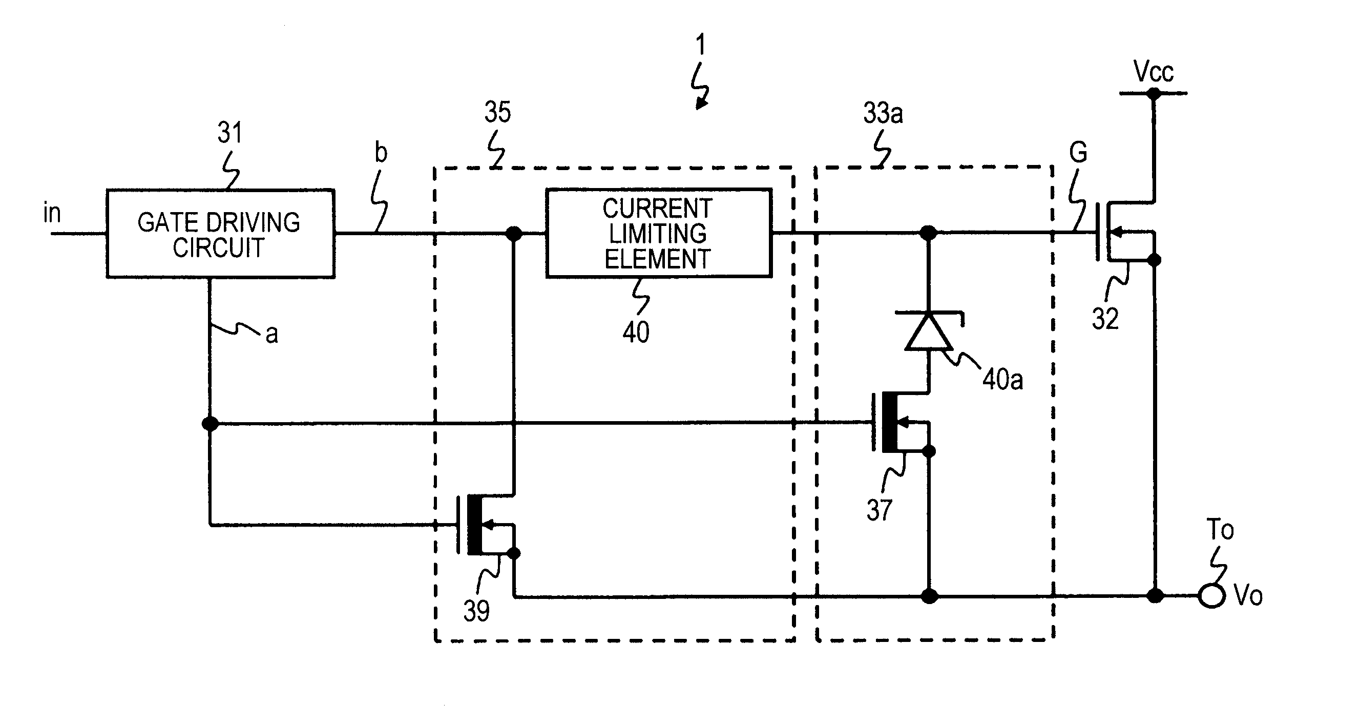
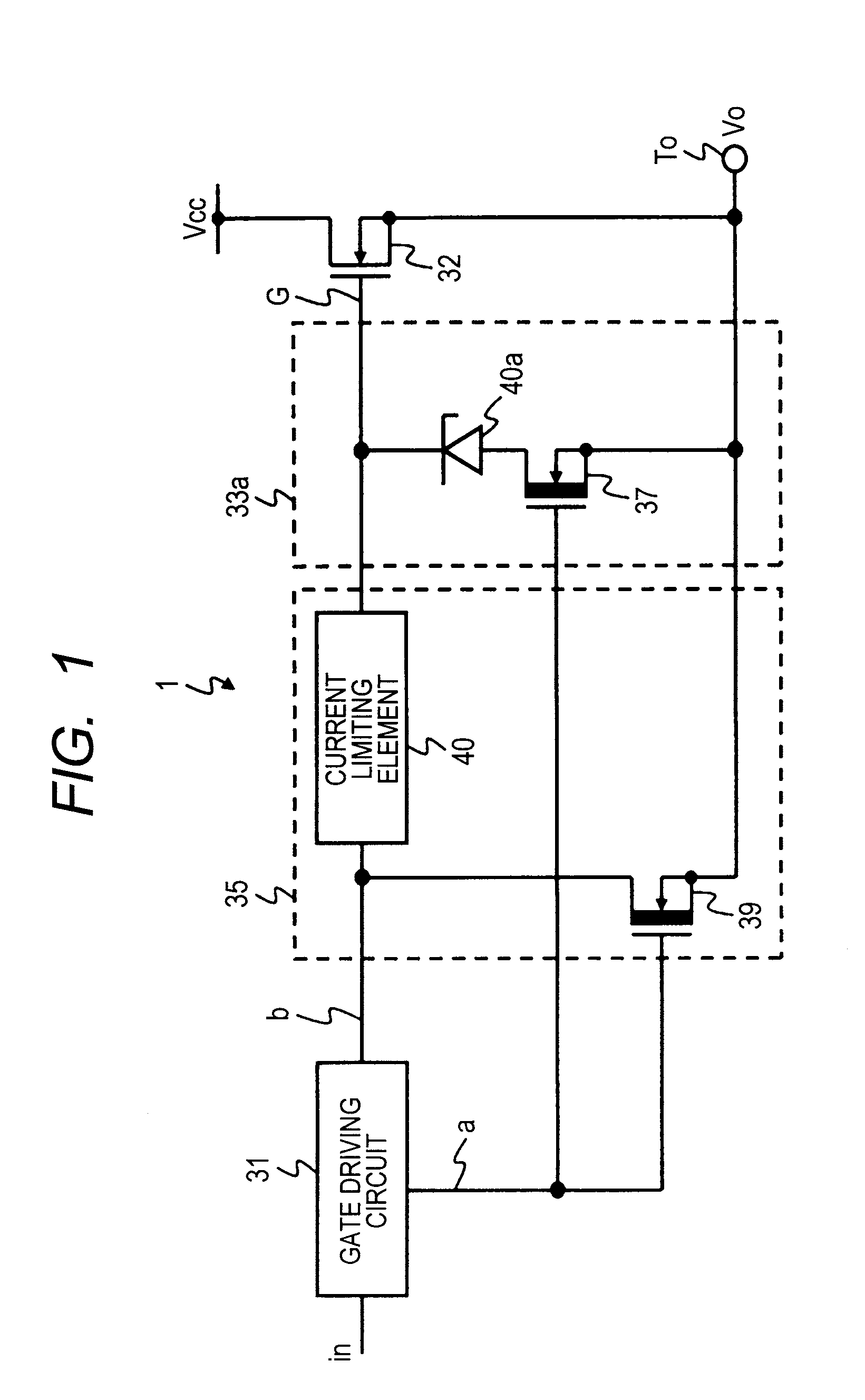
[0030]FIG. 1 illustrates a circuit diagram of a power supply control circuit 1 according to a first embodiment of the present invention. The power supply control circuit 1 illustrated in FIG. 1 comprises a gate driving circuit 31, an output transistor 32, a discharge circuit 33a, and a discharge circuit 35. The discharge circuit 33a comprises a transistor (a first depletion-type N-channel MOS transistor) 37 and a discharge cutoff circuit 40a. The discharge circuit 35 comprises a current limiting element 40 and a transistor (a second depletion-type N-channel MOS transistor) 39. The output transistor 32 is an N-channel MOS transistor. The transistors 37 and 39 are a depletion-type N-channel MOS transistor. A Zener diode 40a is used as the discharge cutoff circuit 40a.
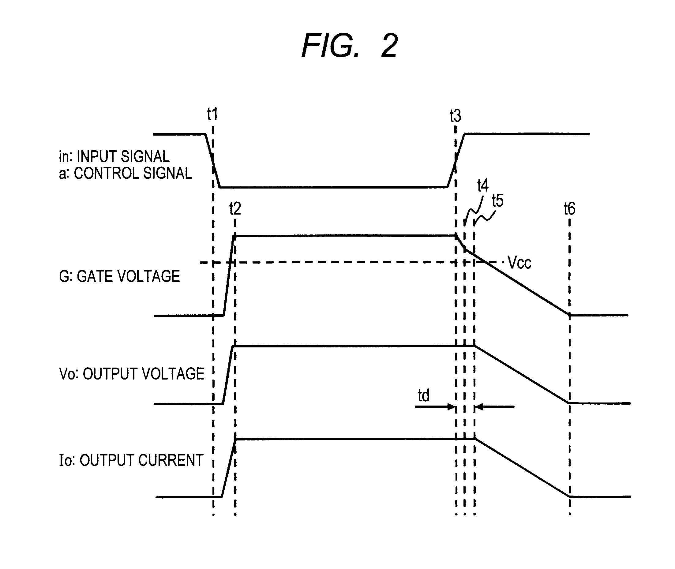
[0031]As for the gate driving circuit 31, an input terminal is coupled to an external input terminal “in”, one output terminal is coupled to a gate of the transistor 39, and another output terminal is coupled to one term...
second embodiment
[0053]FIG. 3 illustrates a circuit diagram of a power supply control circuit 2 according to a second embodiment of the present invention. As compared with the power supply control circuit 1 illustrated in FIG. 1, the power supply control circuit 2 illustrated in FIG. 3 comprises a discharge circuit 33b instead of the discharge circuit 33a. The discharge circuit 33b comprises a transistor 37 and a discharge cutoff circuit 40b. The discharge cutoff circuit 40b comprises plural N-channel MOS transistors 40b1-40bn (n is a natural number), in each of which a gate and a drain are coupled in common. The transistor 40b1-40bn are coupled in series between a gate of the output transistor 32 and a drain of the transistor 37. The other circuit configuration is the same as that of the circuit illustrated in FIG. 1; therefore, the explanation thereof is omitted.
[0054]The power supply control circuit 1 illustrated in FIG. 1 cuts off the first discharge path when the gate voltage G of the output tr...
third embodiment
[0059]FIG. 4 illustrates a circuit diagram of a power supply control circuit 3 according to a third embodiment of the present invention. As compared with the power supply control circuit 1 illustrated in FIG. 1, the power supply control circuit 3 illustrated in FIG. 4 comprises a discharge circuit 33c instead of the discharge circuit 33a. The discharge circuit 33c comprises a transistor 37 and a discharge cutoff circuit 40c. An N-channel MOS transistor 40c is used as the discharge cutoff circuit 40c. As for the transistor 40c, a gate and a drain are coupled in common to a gate of the output transistor 32, and a source is coupled to a drain of the transistor 37. The other circuit configuration is the same as that of the circuit illustrated in FIG. 1; therefore, the explanation thereof is omitted.
[0060]In the second embodiment, a threshold voltage of whether or not to cut off the first discharge path is adjusted as a function of the number of transistors 40b1-40bn. On the other hand, ...
PUM
 Abstract
Description
Claims
Application Information


