Enhanced silicon all-optical modulator

a technology of all-optical modulators and silicon, applied in the field of all-optical modulators, can solve the problems of severe limitations in the approach, weak effects, and high peak optical power levels for modulation

Inactive Publication Date: 2011-07-07
UNIV OF WASHINGTON CENT FOR COMMERICIALIZATION
View PDF4 Cites 1 Cited by
  • Summary
  • Abstract
  • Description
  • Claims
  • Application Information

AI Technical Summary

Benefits of technology

[0016]In one embodiment, a material providing single-photon absorption is an alloy of one or more of silicon, germanium, and tin, in one embodiment, the material providing single-photon absorption comprises a dopant. In one embodiment, the optical modulator comprises a junction selected from a P-N junction and a P-I-N junction.

Problems solved by technology

Both effects are weak in silicon, and require extremely high (˜5 W) peak optical power levels to achieve modulation.
This approach has severe limitations.
Because of the disparate wavelengths for gate and signal, these devices cannot be cascaded into circuits that require feedback.

Method used


Image

  • Enhanced silicon all-optical modulator
  • Enhanced silicon all-optical modulator
  • Enhanced silicon all-optical modulator

Examples


Embodiment Construction

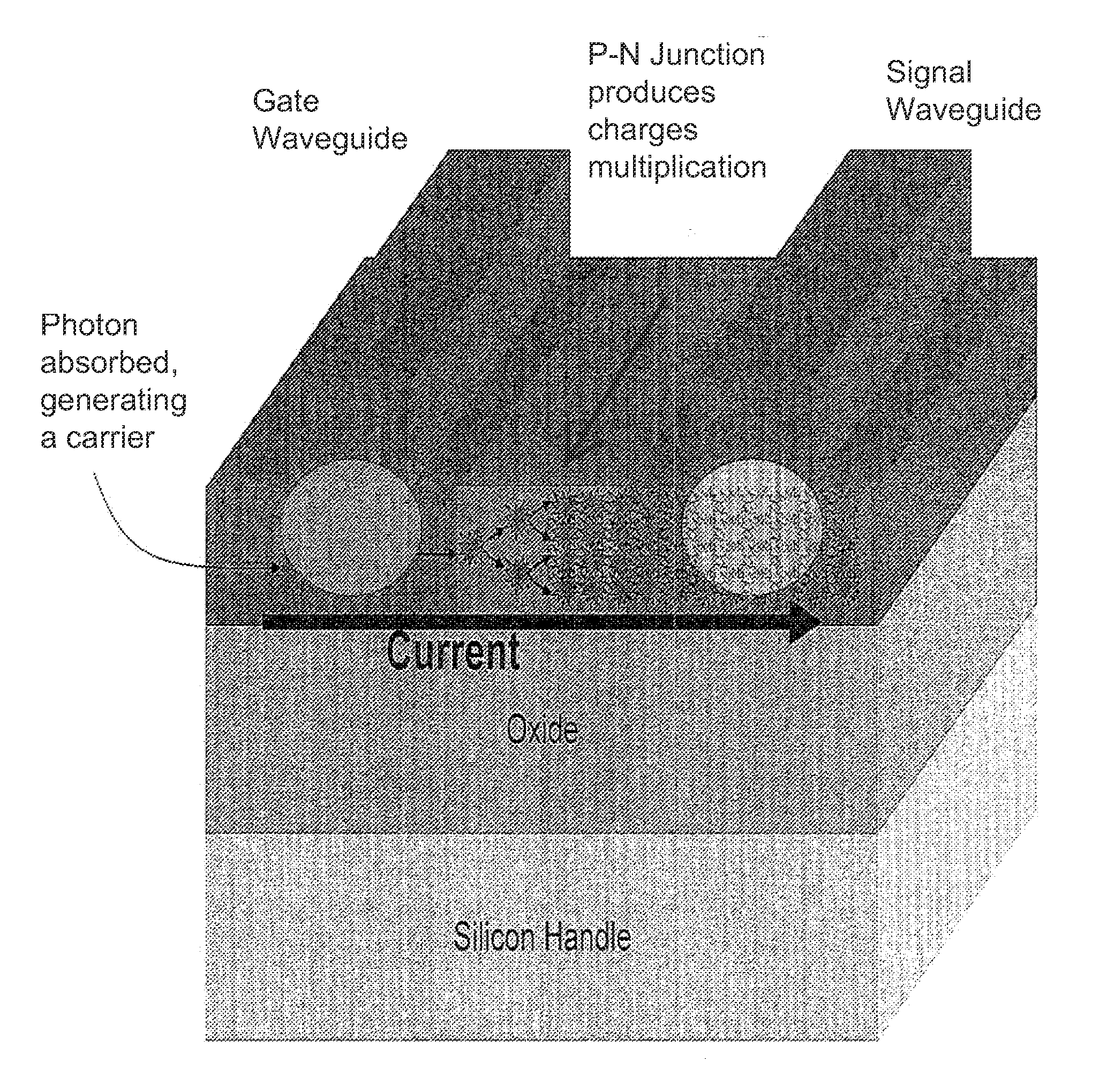
[0045]Because silicon has a bandgap of 1.12 eV, it is an ideal material platform for near-infrared integrated optical circuits. Electrically driven modulation and an optically pumped silicon laser have been previously demonstrated. For all-optical signal processing applications, low-power all-optical modulation is very useful and would represent an appreciable advance. Applications that are contemplated include optical buffering, all-optical wavelength conversion, and all-optical computation.

[0046]Silicon is an extremely attractive material platform for integrated optics at telecommunications wavelengths, particularly for integration with CMOS circuits. Developing detectors and electrically pumped lasers at telecom wavelengths are the two main technological hurdles before silicon can become a comprehensive platform for integrated optics. We describe a photocurrent in unimplanted SOI ridge waveguides. It is believed that the photocurrent is a consequence of surface state absorption. ...


PUM

PropertyMeasurementUnit
lengthaaaaaaaaaa
frequencyaaaaaaaaaa
frequencyaaaaaaaaaa

Abstract

A single-photon absorption all-optical signal-processing device, systems employing the same, and methods of making and using the same. Illustrative examples are provided based on silicon semiconductor technology that employs rectangular waveguides fabricated on SOI wafers. In some embodiments, it is observed that the waveguides have surface state density, σ, of not less than 1.5×1018 cm−1s−1mW−1 to provide a single-photon absorption operation mode. In some embodiments, some portion of the ridge waveguide structure has a surface to volume ratio of at least 18 μm−1, computed using a unit length of 1 μm of the waveguide, with the width and depth dimensions of the waveguide being measured in units of microns.

Description

CROSS-REFERENCE TO RELATED APPLICATIONS[0001]This application claims priority to and the benefit of co-pending U.S. provisional patent application Ser. No. 61 / 027,022, filed Feb. 7, 2008, which application is incorporated herein by reference in its entirety.STATEMENT REGARDING FEDERALLY FUNDED RESEARCH OR DEVELOPMENT[0002]The U.S. Government has certain rights in this invention pursuant to Grant No, HR0011-04-1-0054 awarded by DARPA and Grant No. FA9550-04-1-0434 awarded by AFOSR.FIELD OF THE INVENTION[0003]The invention relates to all-optical modulators in general and particularly to a silicon all-optical modulator that employs single photon absorption.BACKGROUND OF THE INVENTION[0004]All-optical, low-power modulation is a major goal in photonics. Because of their high mode-field concentration and ease of manufacturing, nanoscale silicon waveguides offer an intriguing platform for photonics. To the best knowledge and belief of the inventor, all-optical modulators built with silicon...

Claims


Application Information

Patent Timeline
Patent Type & Authority Applications(United States)
IPC IPC(8): G02F1/035
CPCG02F1/025G02F2001/0152G02F1/2257G02F1/0152
Inventor HOCHBERG, MICHAEL J.BAEHR-JONES, THOMAS W.
Owner UNIV OF WASHINGTON CENT FOR COMMERICIALIZATION
Why Eureka
Try Eureka