Reclamation of scrap materials for LED manufacturing

a scrap material and led manufacturing technology, applied in the field of reclamation of scrap materials, can solve the problems of substrate loss and high cost of substrates

Inactive Publication Date: 2011-07-14
APPLIED MATERIALS INC
View PDF7 Cites 24 Cited by
  • Summary
  • Abstract
  • Description
  • Claims
  • Application Information

AI Technical Summary

Benefits of technology

[0010]In one embodiment, a method for fabricating a compound nitride semiconductor structure within desired parameters comprises depositing a first group-III nitride layer over one or more substrates within a first processing chamber, testing the first group-III nitride layer to determine whether the first group-III nitride layer is within the desired parameters, removing at least a portion of the first group-III nitride layer if the first layer is not within the desired parameters, and depositing an additional first group-III nitride layer to replace the removed portion of the first group-III nitride layer.
[0011]In another embodiment, a method for fabricating a compound nitride semiconductor structure within desired parameters comprises depositing a first GaN layer over the one or more substrates within the first processing chamber, testing the first GaN layer within the first processing chamber to determine whether the first GaN layer is within the desired parameters, removing at least a portion of the first GaN layer if the first GaN layer is not within the desired parameters, depositing an additional first GaN layer to replace the removed portion of the first GaN layer within the first processing chamber, depositing an InGaN layer over the one or more substrates within a secon...

Problems solved by technology

In some cases, the quality of the deposited films may not be adequate to form high quality or even operational devices, resulting in the loss of the substrates.
In many...

Method used


Image

  • Reclamation of scrap materials for LED manufacturing
  • Reclamation of scrap materials for LED manufacturing
  • Reclamation of scrap materials for LED manufacturing

Examples


Embodiment Construction

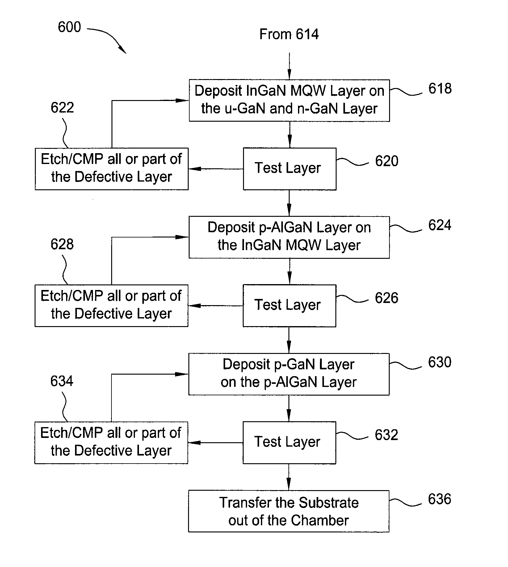
[0022]Embodiments of the invention generally relate to methods for repairing or replacing films or layers of Group III-V materials that may be formed by metal organic chemical vapor deposition (MOCVD) processes and / or hydride vapor phase epitaxial (HVPE) processes. By periodic testing of the layers during the formation process, low-quality layers that may result in low-quality or defective devices may be detected prior to completion of the device. These low-quality layers may be partially or completely removed, and redeposited to reclaim the substrate and any remaining high-quality layers that were previously deposited under the low-quality layer.

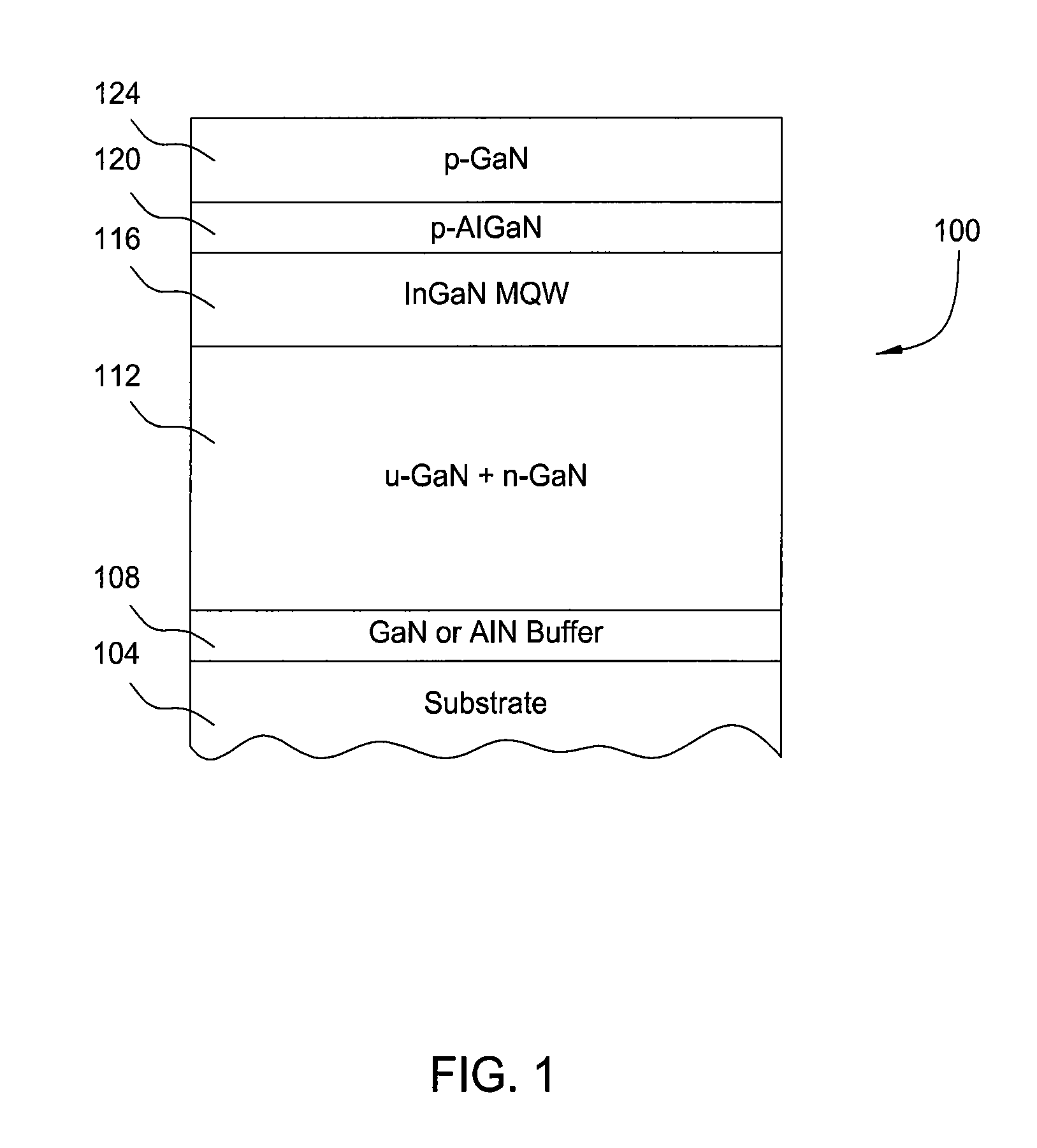
[0023]Currently, metal organic chemical vapor deposition (MOCVD) techniques are the most widely used techniques for the growth of Group III-nitride based LED manufacturing. An exemplary nitride-based structure is illustrated in FIG. 1 as a GaN-based LED structure 100. It is fabricated over a substrate 104. Exemplary substrates include sapph...


PUM

PropertyMeasurementUnit
Semiconductor propertiesaaaaaaaaaa

Abstract

A method for reclamation of scrap materials during the formation of Group III-V materials by metal-organic chemical vapor deposition (MOCVD) processes and/or hydride vapor phase epitaxial (HVPE) processes is provided. More specifically, embodiments described herein generally relate to methods for repairing or replacing defective films or layers during the formation of devices formed by these materials. By periodic testing of the layers during the formation process, low-quality layers that may result in low-quality or defective devices may be detected prior to completion of the device. These low-quality layers may be partially or completely removed and redeposited to reclaim the substrate and any remaining high-quality layers that were previously deposited under the low-quality layer.

Description

CROSS-REFERENCE TO RELATED APPLICATIONS[0001]This application claims benefit of U.S. provisional patent application Ser. No. 61 / 293,462, filed Jan. 8, 2010, which is herein incorporated by reference.BACKGROUND OF THE INVENTION[0002]1. Field of the Invention[0003]Embodiments of the present invention generally relate to the manufacturing of devices, such as light emitting diodes (LED's), laser diodes (LD's) and, more particularly, to processes for reclamation of scrap materials during the manufacturing processes.[0004]2. Description of the Related Art[0005]Group III-V films are finding greater importance in the development and fabrication of a variety of semiconductor devices, such as short wavelength LED's, LD's, and other electronic devices including high power, high frequency, high temperature transistors and integrated circuits. For example, short wavelength (e.g., blue / green to ultraviolet) LED's are fabricated using the Group III-nitride semiconducting material gallium nitride (...

Claims


Application Information

Patent Timeline
IPC IPC(8): H01L21/66H01L21/465H01L21/36
CPCH01L21/0254H01L33/007H01L22/20H01L21/02579
Inventor SU, JIEKRYLIOUK, OLGA
Owner APPLIED MATERIALS INC
Why Eureka
Try Eureka