

Method of manufacturing semiconductor device
a manufacturing method and technology for semiconductor devices, applied in semiconductor devices, semiconductor/solid-state device details, electrical devices, etc., can solve problems such as chip cracking, and achieve the effect of reducing chip cracking
- Summary
- Abstract
- Description
- Claims
- Application Information
AI Technical Summary
Benefits of technology
Problems solved by technology
Method used
Image

Examples
first embodiment
Modifications to First Embodiment
[0265]Description will be given to modifications to the first embodiment.
[0266]FIG. 44 is a perspective view illustrating the structure of a semiconductor device in a first modification to the first embodiment of the invention; FIG. 45 is a perspective view illustrating an example of the structure of the semiconductor device in FIG. 44 on the back surface side; and FIG. 46 is a sectional view illustrating the structure of a semiconductor device in a second modification to the first embodiment of the invention. FIG. 47 is a plan view illustrating the structure of a semiconductor device in a third modification to the first embodiment of the invention with a sealing body seen through; FIG. 48 is a sectional view illustrating an example of a structure obtained by cutting the semiconductor device along line A-A of FIG. 47; and FIG. 49 is a sectional view illustrating an example of a structure obtained by cutting the semiconductor device along line B-B of ...
second embodiment
[0273]FIG. 50 is a plan view illustrating an example of the structure of a semiconductor device in the second embodiment of the invention with a sealing body seen through; FIG. 51 is a sectional view illustrating an example of the structure obtained by cutting the semiconductor device along line A-A of FIG. 50; FIG. 52 is a sectional view illustrating an example of the structure obtained by cutting the semiconductor device along line B-B of FIG. 50; and FIG. 53 is an enlarged partial sectional view illustrating the structure of a semiconductor device in a first modification to the second embodiment of the invention.
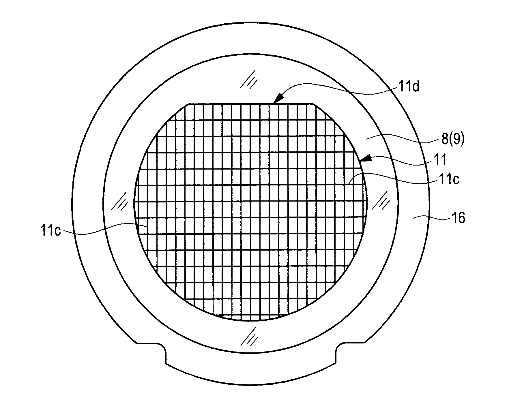
[0274]The semiconductor device in the second embodiment illustrated in FIG. 50 to FIG. 52 is obtained by laminating thin-type semiconductor chips in 16 tiers over a wiring board 3 as the base material as in the first embodiment. The semiconductor device has such a structure that semiconductor chips are laminated by eight tiers with the lamination direction changed by 90 d...
PUM
 Abstract
Description
Claims
Application Information