Thin film solar cell and manufacturing method thereof

a solar cell and thin film technology, applied in the field of solar cells, can solve the problems of difficult effective utilization of light with wavelengths greater than the red light range, ineffective absorption of light, etc., and achieve the effect of improving photoelectric conversion efficiency and enhancing light utilization ra

Inactive Publication Date: 2011-07-21
AURIA SOLAR CO LTD
View PDF4 Cites 11 Cited by
  • Summary
  • Abstract
  • Description
  • Claims
  • Application Information

AI Technical Summary

Benefits of technology

[0008]The present invention provides a thin film solar cell to enhance the light utilization rate and further improve the photoelectric conversion efficiency.
[0037]In view of the above, the thin film solar cell of the present invention has a first adhesive layer and a reflective layer, and the surface of the first adhesive layer in contact with the reflective layer has a texture structure to reflect the light beam. Accordingly, the light paths of the light beam passing the photovoltaic layer are increased, and the possibility of the light beam absorbed by the photovoltaic layer is enhanced. In other words, the thin film solar cell of the present invention has higher photoelectric conversion efficiency. In addition, the present invention also provides a manufacturing method to form the above-mentioned thin film solar cell.

Problems solved by technology

The light path of the light passing the photovoltaic layer is limited by the thickness of the photovoltaic layer, so that the light can not be effectively absorbed.
Specially, the light with wavelengths greater than the red light range is difficult to be utilized effectively.

Method used


Image

  • Thin film solar cell and manufacturing method thereof
  • Thin film solar cell and manufacturing method thereof
  • Thin film solar cell and manufacturing method thereof

Examples


Embodiment Construction

[0050]Reference will now be made in detail to the present preferred embodiments of the invention, examples of which are illustrated in the accompanying drawings. Wherever possible, the same reference numbers are used in the drawings and the description to refer to the same or like parts.

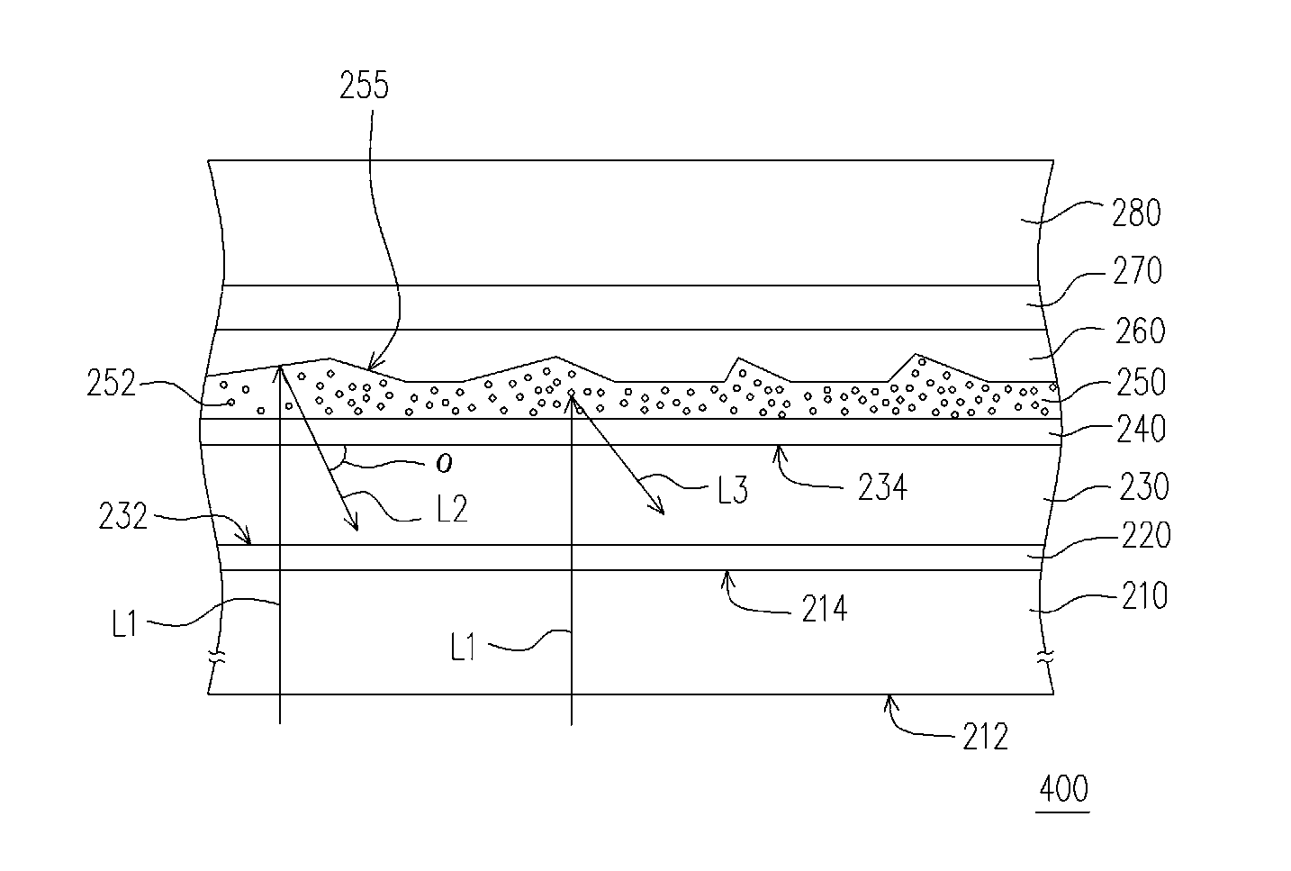
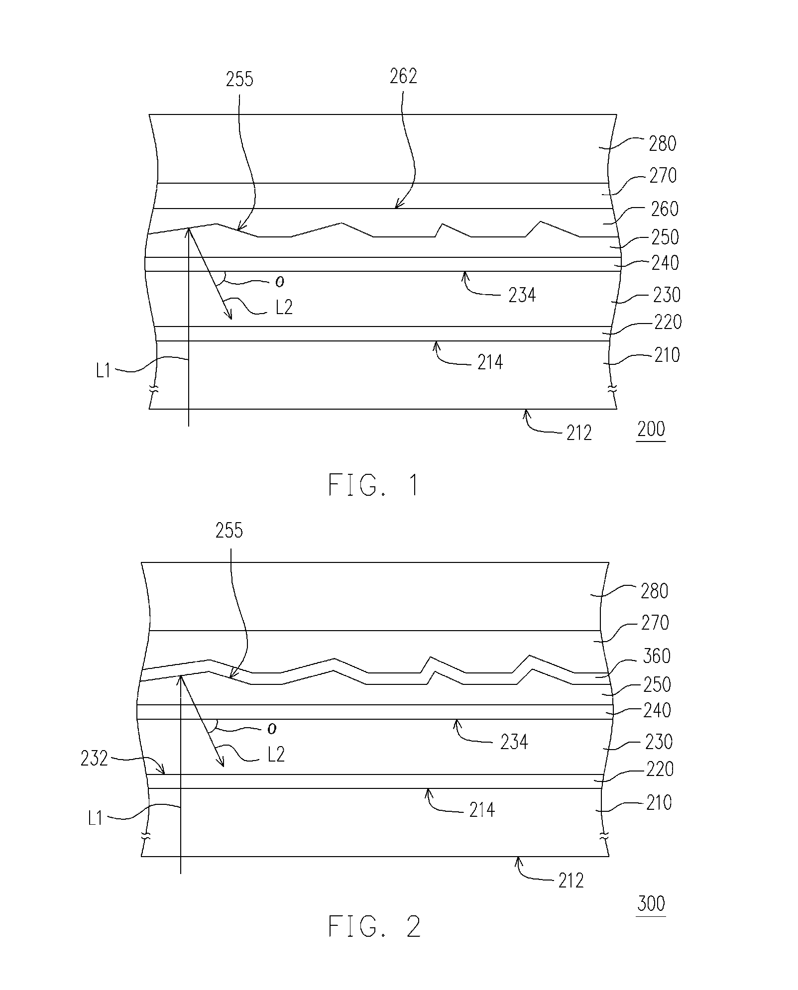
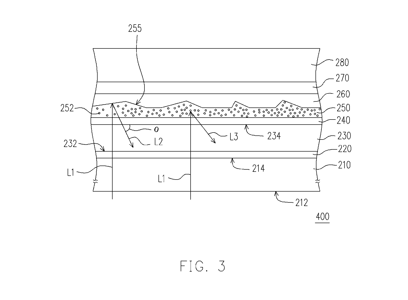
[0051]FIG. 1 schematically illustrates a cross-sectional view of an embodiment of a thin film solar cell according to the present invention. Referring to FIG. 1, the thin film solar cell 200 of the present invention includes a transparent substrate 210, a first transparent conductive layer 220, a photovoltaic layer 230, a second transparent conductive layer 240, a first adhesive layer 250 and a reflective layer 260.

[0052]The transparent substrate 210 has a light incident surface 212 and a back surface 214 opposite to the light incident surface 212. This embodiment in which the transparent substrate 210 is a glass substrate is provided for illustration purposes, and is not construed as limiting the pr...


PUM


Abstract

A thin film solar cell includes a transparent substrate, a first transparent conductive layer, a photovoltaic layer, a second transparent conductive layer, a first adhesive layer and a reflective layer is provided. The first transparent conductive layer is disposed on a back surface of the transparent substrate. The photovoltaic layer is disposed on the first transparent conductive layer. The second transparent conductive layer is disposed on the photovoltaic layer. The first adhesive layer is disposed on the second transparent conductive layer. The reflective layer is disposed on the first adhesive layer. The surface of the first adhesive layer in contact with the reflective layer is a texture structure. The light beam passing the first adhesive layer is reflected by the texture structure or the reflective layer and transmitted back to the photovoltaic layer, and the wavelength range of the reflected light beam is substantially between 600 nm and 1,100 nm.

Description

CROSS-REFERENCE TO RELATED APPLICATIONS[0001]This non-provisional application claims priority under 3535 U.S.C. §119(a) on Patent Application No. 099107827 filed in Taiwan, R.O.C. on Mar. 17, 2010, the entire contents of which are hereby incorporated by reference.BACKGROUND OF THE INVENTION[0002]1. Field of Invention[0003]The present invention relates to a solar cell and a manufacturing method thereof, and more particularly to a thin film solar cell with higher photoelectric conversion efficiency and a manufacturing method thereof.[0004]2. Description of Related Art[0005]Solar cells have drawn attention in many alternative energy and renewable energy technologies. The main reason is that solar cells can collect electricity directly from sunlight, and carbon dioxide, nitride gas or pernicious gases are not generated during the electricity generation process, so that the environment is not polluted. In various solar cells, a thin film solar cell has strong development potential due to...

Claims


Application Information

Patent Timeline
Patent Type & Authority Applications(United States)
IPC IPC(8): H01L31/0232H01L31/18
CPCH01L31/0296H01L31/0304H01L31/03685H01L31/03687H01L31/03762H01L31/056Y02E10/52Y02E10/544Y02E10/545Y02E10/548H01L31/03765Y02P70/50
Inventor TSAI, CHIN-YAO
Owner AURIA SOLAR CO LTD
Why Eureka
Try Eureka