

Semiconductor device and electronic device
a semiconductor and electronic technology, applied in the field of semiconductor devices, can solve the problems of complex structure of the driver circuit, difficult for the transistor including amorphous silicon to drive at high frequencies, and difficult for the transistor including single crystal silicon or polycrystalline silicon to be formed by a low-temperature process
- Summary
- Abstract
- Description
- Claims
- Application Information
AI Technical Summary
Benefits of technology
Problems solved by technology
Method used
Image

Examples
embodiment 1
[0033]In this embodiment, a semiconductor device which is an embodiment of the present invention is described with reference to FIGS. 1A to 1C, FIGS. 2A and 2B, FIGS. 3A and 3B, FIGS. 4A to 4C, FIGS. 5A and 5B, FIGS. 6A and 6B, and FIG. 7.
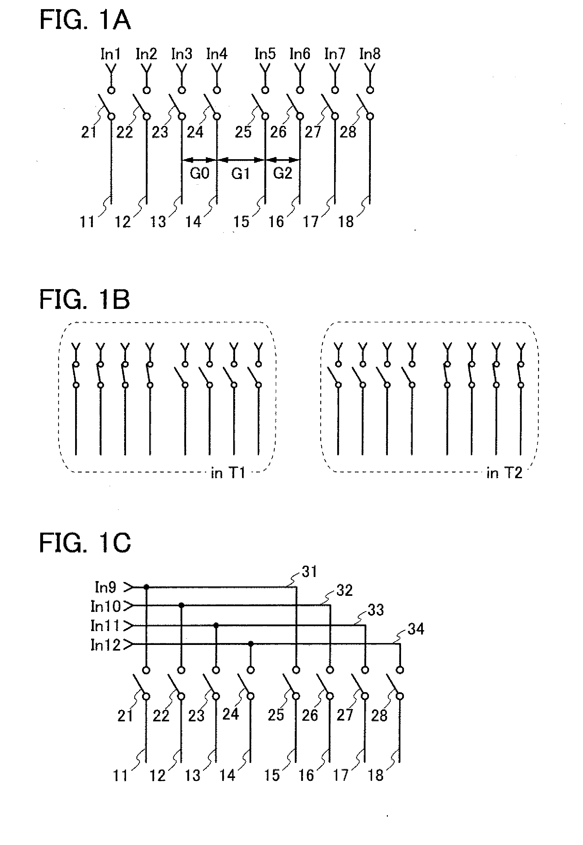
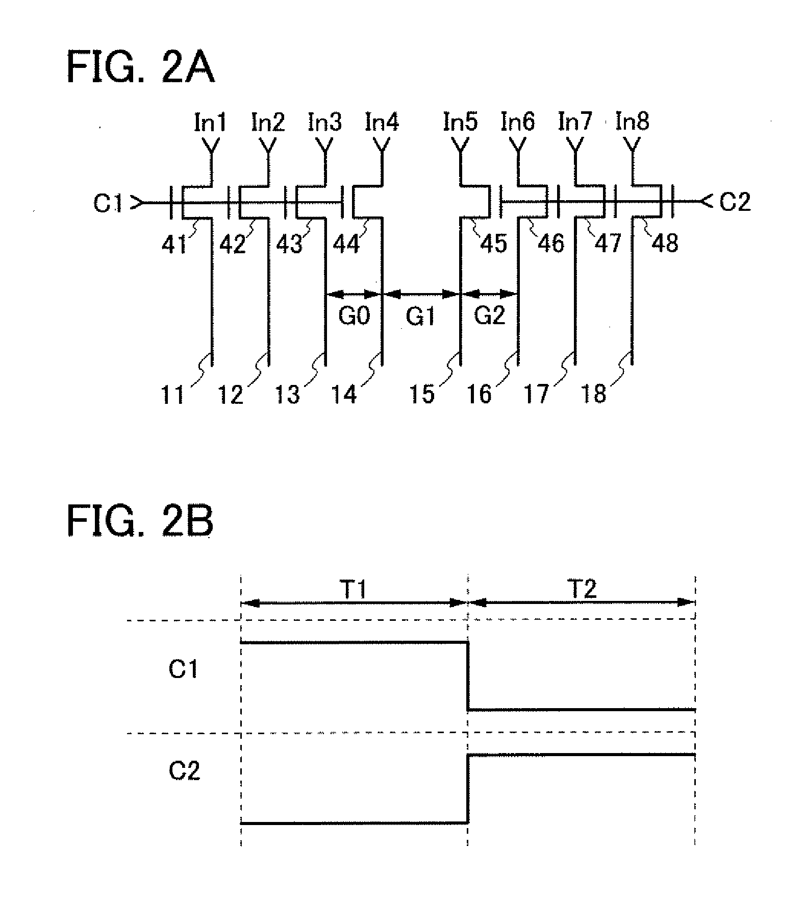
[0034]FIG. 1A illustrates positions of a plurality of signal lines 11 to 18 and a plurality of switches 21 to 28 which control input of a signal to the plurality of signal lines 11 to 18, which are included in a semiconductor device of this embodiment. Note that the switch 21 controls supply of an input signal (In1) to the signal line 11. Similarly, the switches 22 to 28 control supply of input signals (In2 to In8) to the signal lines 12 to 18. In addition, the plurality of signal lines 11 to 18 are arranged parallel or approximately parallel to one another. Further, a distance between the signal line 14 and the signal line 15 (G1) is longer than a distance between the signal line 13 and the signal line 14 (G0) and longer than a distance between th...
embodiment 2
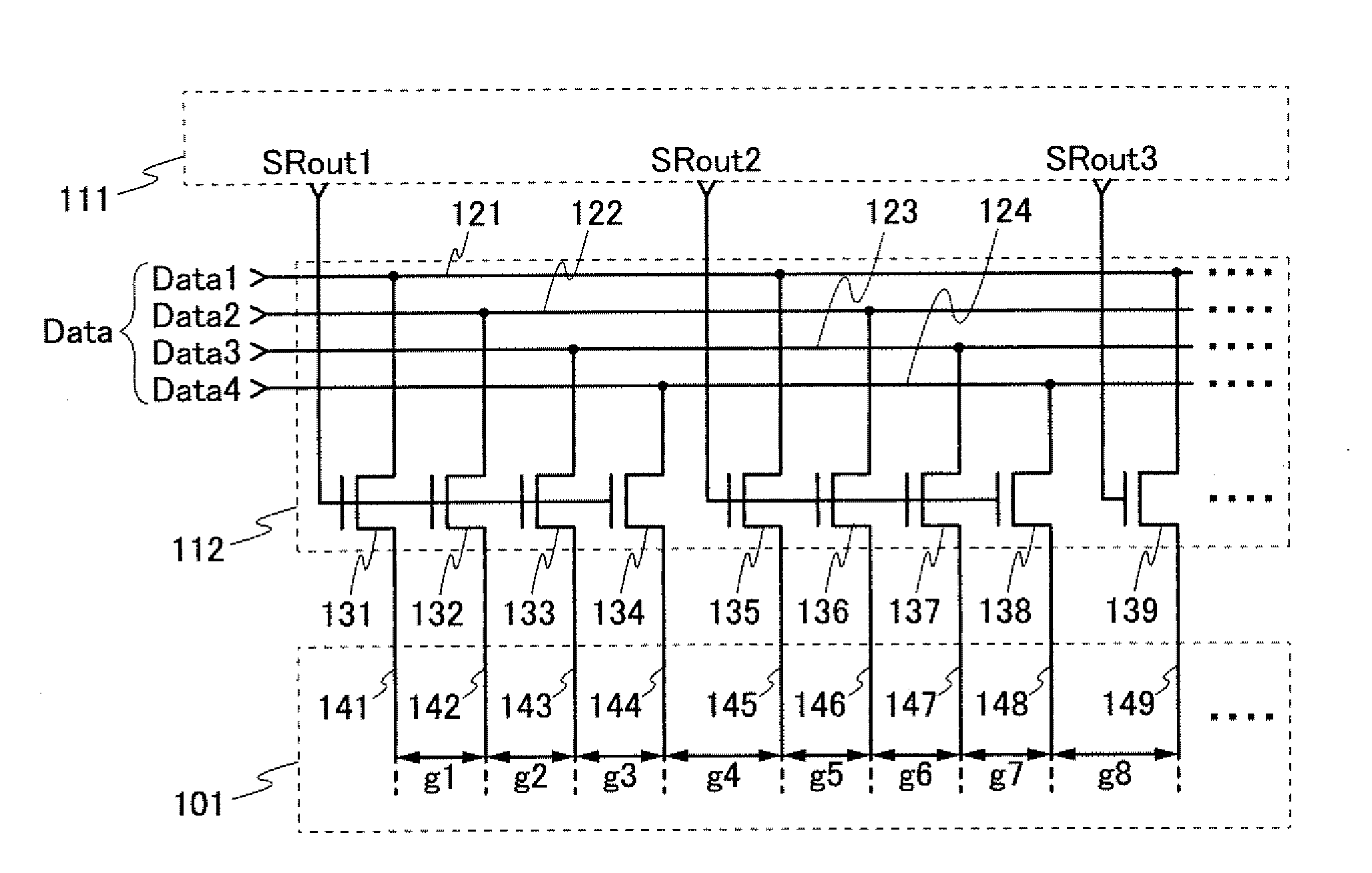
[0057]In this embodiment, a semiconductor device of an embodiment of the present invention is described. Specifically, an example of an active matrix display device which performs data division driving is described with reference to FIGS. 8A and 8B, FIGS. 9A and 9B, FIG. 10, FIG. 11, and FIG. 12.
[0058]FIG. 8A illustrates a structure example of an active matrix display device. A display device illustrated in FIG. 8A includes a pixel portion 101, a source signal line driver circuit 102, a gate signal line driver circuit 103, a plurality of source signal lines 104 which are arranged in parallel or approximately parallel, and a plurality of gate signal lines 105 which are arranged in parallel or approximately parallel. The pixel portion 101 includes a plurality of pixels 107. Note that the plurality of pixels 107 are arranged in matrix. Each of the plurality of source signal lines 104 is electrically connected to pixels in any column of the plurality of pixels arranged in matrix, and ea...
embodiment 3
[0083]In this embodiment, an example of a transistor included in the semiconductor device described in Embodiment 1 or Embodiment 2 will be described. Specifically, examples of a structure of a transistor whose channel formation region is formed using an oxide semiconductor and a method for manufacturing the transistor are described with reference to FIGS. 13A to 13D.
[0084]FIGS. 13A to 13D illustrate examples of a specific structure and a process for manufacturing the transistor in Embodiment 1. Note that a transistor 410 illustrated in FIG. 13D has a bottom-gate structure called a channel-etched type and is also referred to as an inverted-staggered transistor. Although a single-gate transistor is illustrated in FIG. 13D, a multi-gate transistor including a plurality of channel formation regions can be formed as needed.
[0085]A process for manufacturing the transistor 410 over a substrate 400 is described below with reference to FIGS. 13A to 13D.
[0086]First, a conductive film is form...
PUM
 Abstract
Description
Claims
Application Information