Memory having a disabling circuit and method for disabling the memory

Active Publication Date: 2011-07-21
ETRON TECH INC
View PDF1 Cites 2 Cited by
  • Summary
  • Abstract
  • Description
  • Claims
  • Application Information

AI Technical Summary

Problems solved by technology

However, it is still possible for the NG parts to be mistakenly packaged.
Although the parameters of the final test is designed to be tighter than the probe test, the NG parts may still pass the final test due to issues such as testing hardware, testing

Method used


Image

  • Memory having a disabling circuit and method for disabling the memory
  • Memory having a disabling circuit and method for disabling the memory
  • Memory having a disabling circuit and method for disabling the memory

Examples


Example

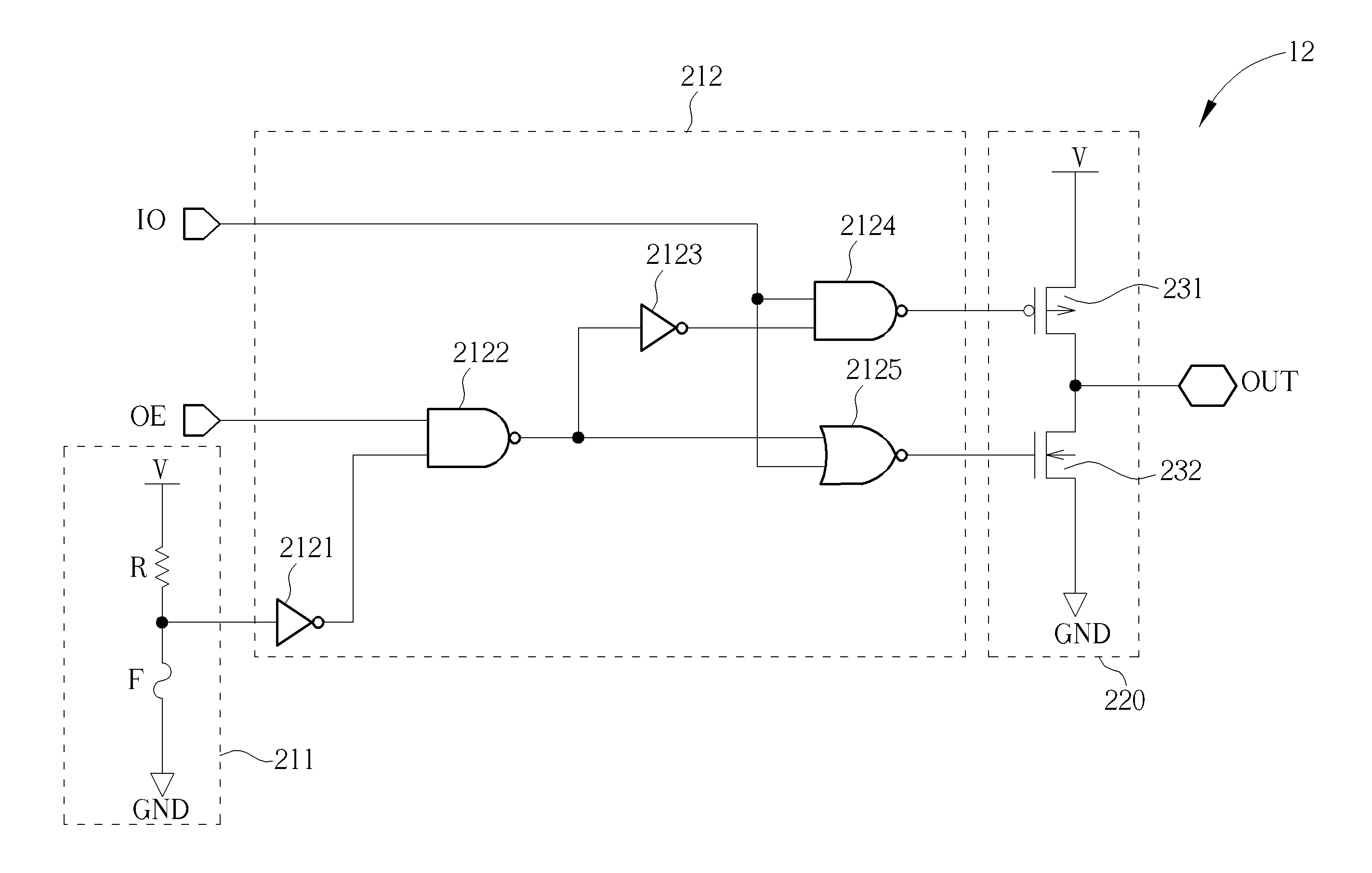
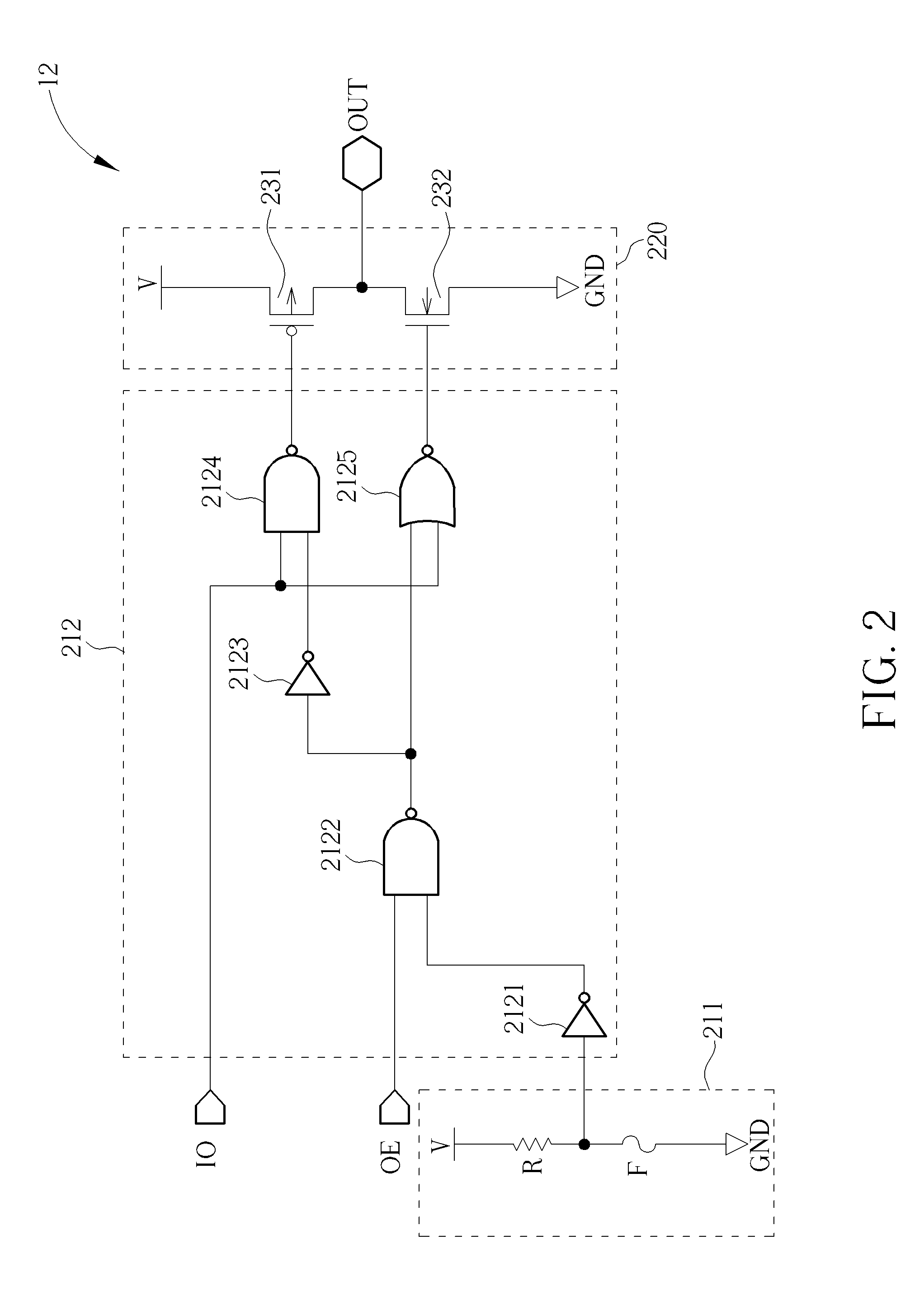
[0014]Therefore, the present invention utilizes a disabling circuit to control the output of a memory. When any memory units of a memory matrix of the memory is classified as an NG part, the disabling circuit outputs a tri-state (e.g. high impedance) to the output end of the memory matrix, effectively “removing” the output of the memory. This way, in the subsequent testing or processing, the memory cannot be accessed and can be identified as an NG part straight away.

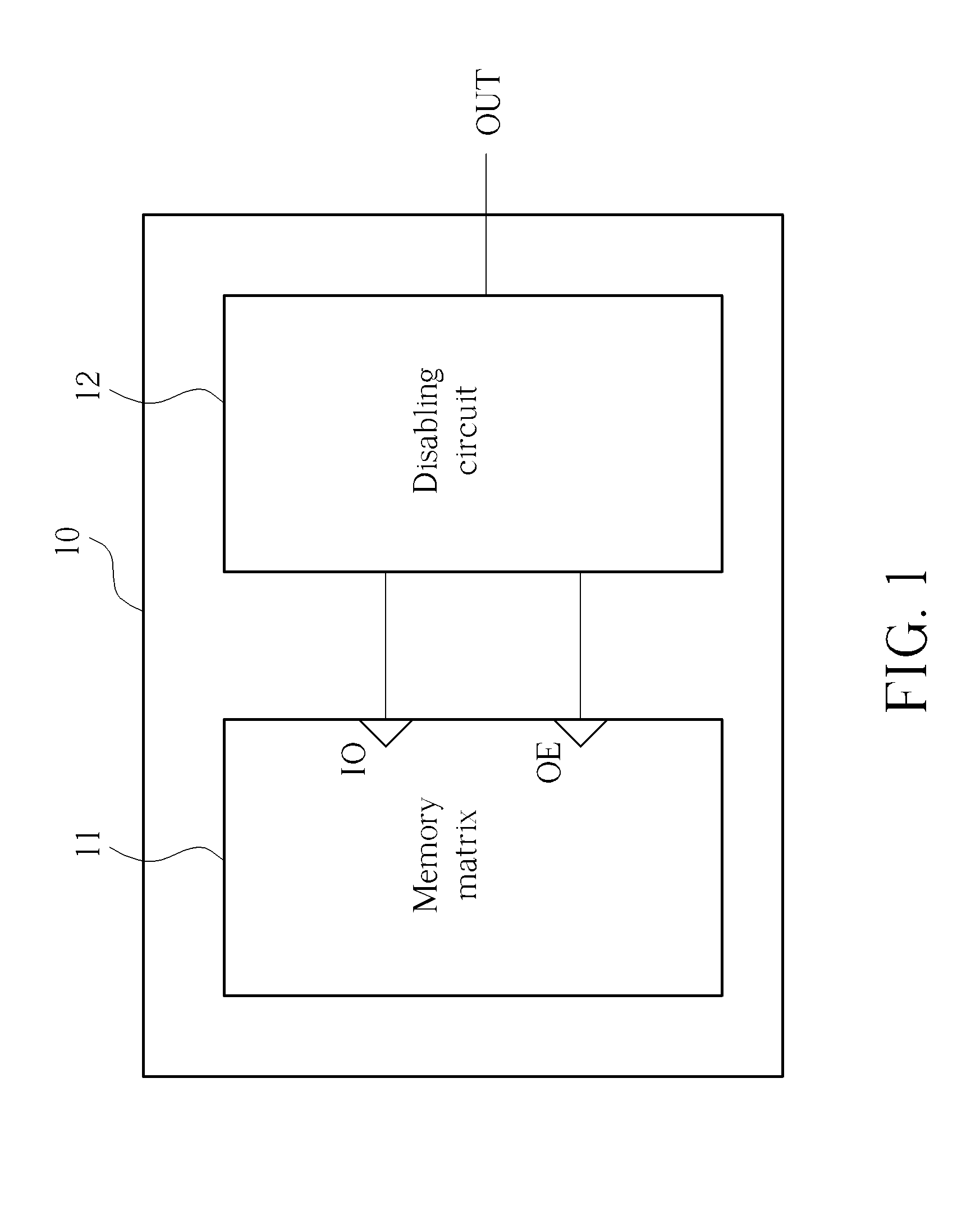
[0015]Please refer to FIG. 1. FIG. 1 is a diagram illustrating the memory 10 of the present invention. Memory 10 comprises a memory matrix 11, a disabling circuit 12 and an output end OUT. The disabling circuit is coupled to a data input / output end IO and an output enable end OE of the memory matrix 11 at the same time. The memory matrix 11 comprises a plurality of memory units; the data stored in the memory units are transmitted to the output end OUT through the disabling circuit 12. The disabling circuit 12 is able to ...


PUM


Abstract

A memory with disabling circuit includes a memory matrix and a disabling circuit. The memory matrix includes a data input/output end and an output enable end. The disabling circuit includes a fuse and an output end. When the fuse is not blown, the disabling circuit transmits the signal of the data input/output end to the output end according to the signal of the output enable end. When the fuse is blown, the disabling circuit generates a tri-state to the output end. Therefore, external circuits cannot perform actions of reading or writing to access the memory matrix.

Description

BACKGROUND OF THE INVENTION[0001]1. Field of the Invention[0002]The present invention is related to a memory, and more particularly, to a memory with a disabling circuit for disabling the memory when the memory is defined as a NG (Not Good) part.[0003]2. Description of the Prior Art[0004]Semiconductor chips, for applications such as memory, have been made from wafers of semiconductor material whereby each wafer is split up into a plurality of dies. During the manufacture process, the wafer undergoes a number of micro-fabrications such as doping, etching, deposition of various materials and photolithographic patterning. Subsequently the wafer is then diced and further packaged.[0005]Generally, wafer testing is performed before the wafer is sent to die preparation / packaging. The process of wafer testing in general can be referred to in several types such as Wafer Sort (WS), Wafer Final Test (WFT), Electronic Die Sort (EDS) and Circuit Probe (CP). During wafer testing all dies present ...

Claims


Application Information

Patent Timeline
IPC IPC(8): G11C17/16
CPCG11C17/16G11C17/18G11C29/1201G11C29/006G11C29/832
Inventor WANG, SHIH-HSINGYUAN, DER-MIN
Owner ETRON TECH INC
Why Eureka
Try Eureka