

Galvanic isolator
a galvanic isolator and optical technology, applied in the direction of coils, electric variable regulation, transmission line coupling arrangements, etc., can solve the problems of electrical inefficiency of circuits, hazard to the receiving circuit or individuals in contact with the receiving circuit,
- Summary
- Abstract
- Description
- Claims
- Application Information
AI Technical Summary
Benefits of technology
Problems solved by technology
Method used
Image

Examples
Embodiment Construction
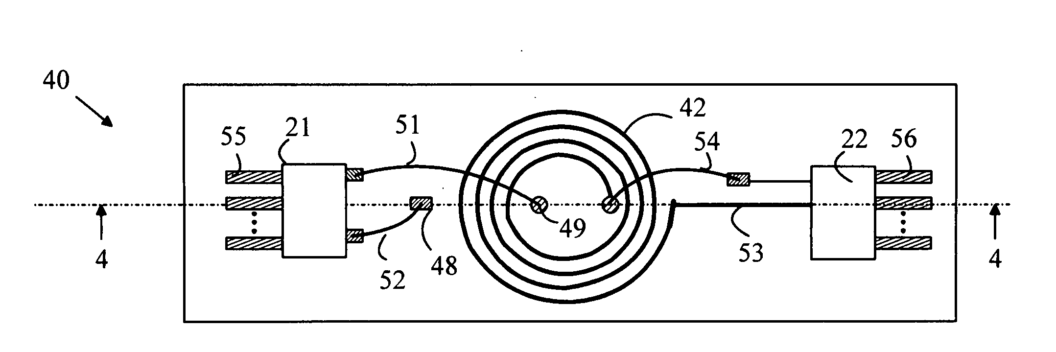
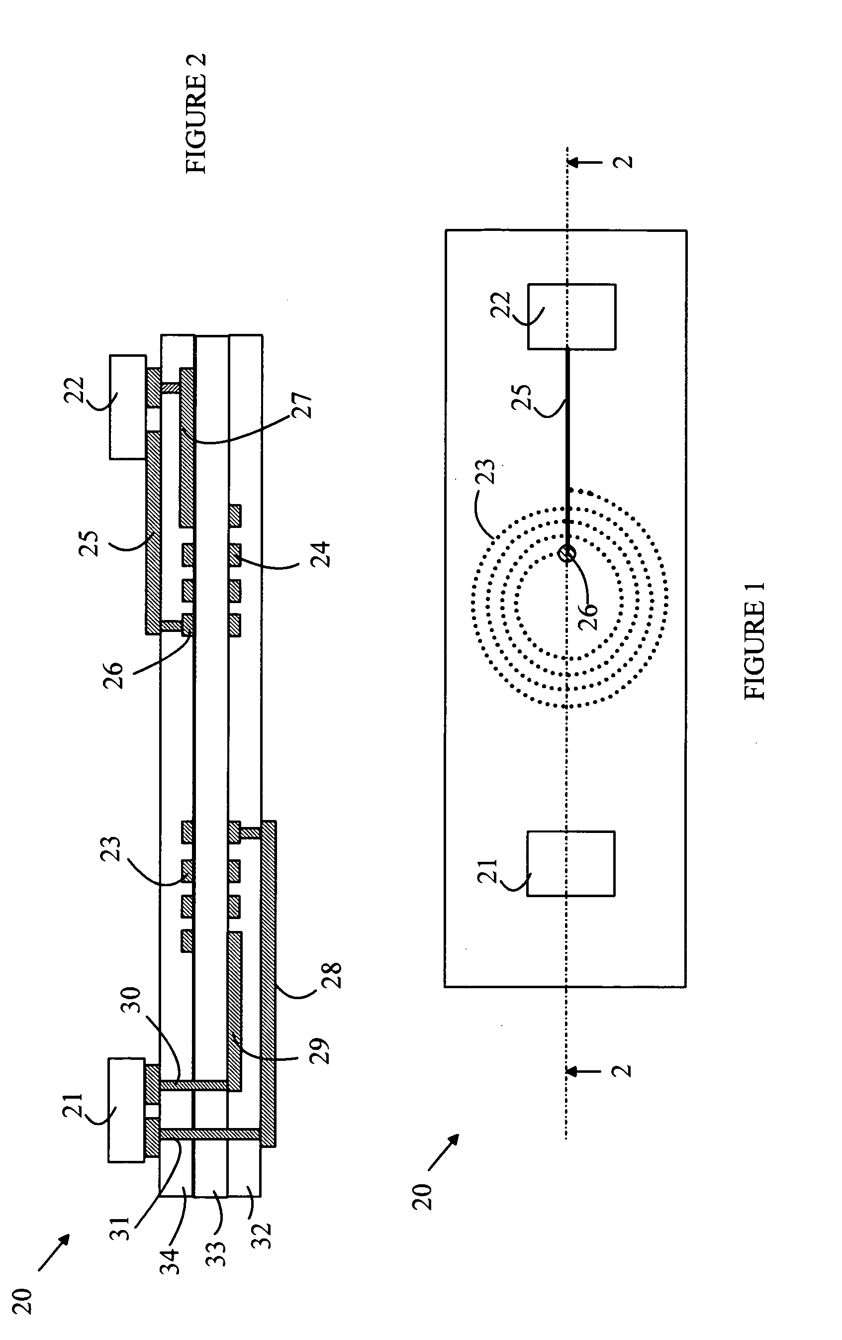
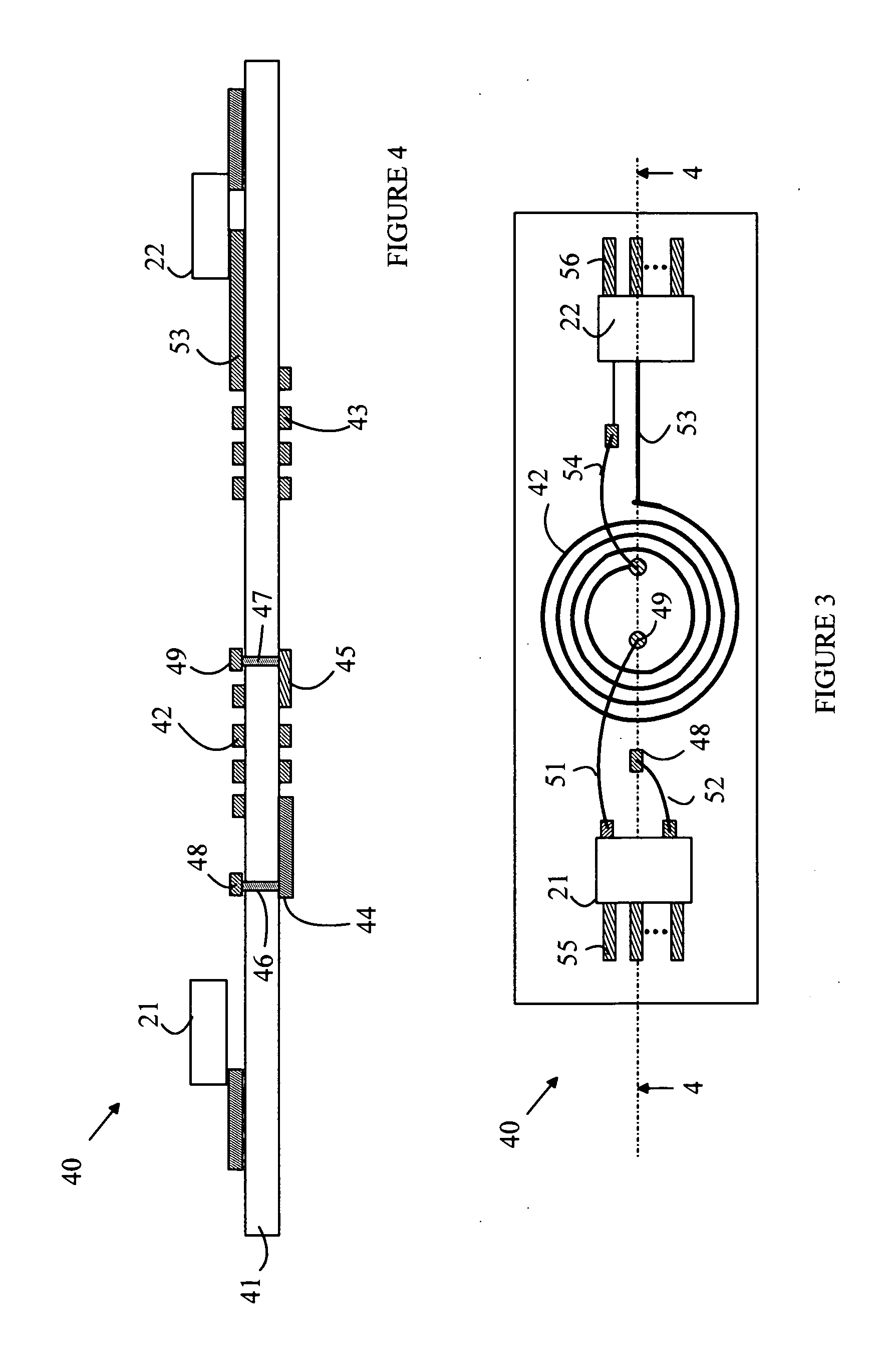
[0018]The manner in which the present invention provides its advantages can be more easily understood with reference to FIGS. 1 and 2, which illustrate one embodiment of a galvanic isolator according to the present invention. FIG. 1 is a top view of galvanic isolator 20, and FIG. 2 is a cross-sectional view of galvanic isolator 20 through line 2-2. Galvanic isolator 20 is includes a transmitter chip 21 and a receiver chip 22 that are bonded to a substrate in which coils 23 and 24 have been fabricated and connected to bond pads on the top surface of layer 34. Alternatively, transmitter chip 21 and receiver chip 22 may be attached to a lead frame and connected by wire bonds to bond pads attached to coils 23 and 24. Other packaging embodiments are possible as well. Coils 23 and 24 form a transformer. The transformer coils are fabricated by lithographically patterning metal layers on the surface of a polymeric substrate 33 that has sufficient thickness and insulation characteristics to ...
PUM
 Abstract
Description
Claims
Application Information